Getting into way too much detail with the Z80 netlist simulation
TL;DR: a detailed look at Z80 instruction timings with the help of a Z80 netlist simulation.
Table of Content
- Table of Content
- Intro
- The shape of Z80 instructions
- General Instruction Timing
- Overlapped Execution
- The 3 Instruction Subsets
- The 2-3-3 Opcode Bit Pattern
- Main Instructions
- Prefix Instruction Overview
- DD and FD Prefixes
- ED Prefix
- CB Prefix
- DD CB and FD CB Prefix
- Interrupt Behaviour
Intro
This is part one of a two-part series about a new cycle-stepped Z80 emulator I wrote recently. In the first post I’ll mainly take a look at the oddities and irregularities in the Z80 instruction set with the help of the Z80 netlist simulation from visual6502.org which I integrated into my own ‘remix’ before starting to work on the actual CPU emulator:
https://floooh.github.io/visualz80remix/
The ‘remix’ has some usability advantages over the original:
- rendering and UI performance is much improved via WASM, WebGL and Dear ImGui
- an integrated assembler simplifies program input
- a tracelog window which shows more information and allows to ‘rewind’ the simulation
There’s a lot more information in the project readme here: https://github.com/floooh/v6502r.
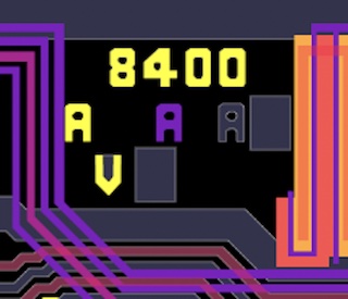
A word of warning though, the Z80 netlist from visual6502 has some subtle differences in undocumented behaviour from what’s known about original Z80s (see here for a list of issues I found so far: https://github.com/floooh/v6502r/issues/2. My guess is that the netlist has been created from a Z8400 because of those two details found on the die:
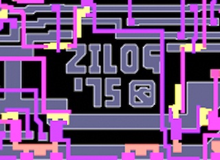
…at least this might explain why the netlist doesn’t suffer from the six ‘reverse engineering traps’ that were placed on the original Z80. By the time the Z8400 was created, the Z80 had already been widely cloned so reverse engineering probably was no longer a concern.
Anyway, back to the actual topic of the blog post:
The Z80 has probably the most messy and irregular instruction set of the popular 8-bit CPUs (certainly when compared to the MOS 6502 or Motorola 6800). The reason is that the Z80 had to be binary compatible with the Intel 8080. While the 8080 has a reasonably clean and structured instruction set, the only way for the Z80 to add new instructions while remaining 8080-compatible was to fill the ‘gaps’ in the 8080 instruction set.
This is why the Z80 instruction set looks clean and structured only in some places (mainly those inherited from the 8080), while at the same time being peppered with seemingly random new Z80-specific instructions. This was the right approach to create an “8080 killer”, but nearly half a century later it makes life a lot harder for emulator authors :)
The shape of Z80 instructions
Like on the Intel 8080, instructions are made up of one or multiple bytes, where the first byte is always the opcode byte.
This simple rule is also true for the Z80-specific ‘prefixed instructions’, which superficially seem to have two opcode bytes. But as we’ll see later, instruction prefixes are actually complete instructions on their own which just influence how the following opcode byte is decoded.
Prefixes aside, there are only three basic instruction ‘shapes’:
Just the opcode byte (for example NOP, LD A,B, RET):
┏━━━━━━━━┓
┃ OPCODE ┃
┗━━━━━━━━┛
    C9      => RET
An opcode byte followed by an 8-bit ‘immediate value’ (for example LD A,n, ADD n, JR d):
┏━━━━━━━━┳━━━━━━┓
┃ OPCODE ┃ IMM8 ┃
┗━━━━━━━━┻━━━━━━┛
    3E      11      => LD A,11h
An opcode byte followed by a 16-bit immediate value (in little endian order): LD HL,nnnn, CALL nn):
┏━━━━━━━━┳━━━━━━━━━┳━━━━━━━━━┓
┃ OPCODE ┃ IMM16LO ┃ IMM16HI ┃
┗━━━━━━━━┻━━━━━━━━━┻━━━━━━━━━┛
    21       34         12      => LD HL,1234h
Instructions that have been ‘modified’ by the DD or FD prefix may come in two additional shapes where an offset byte is inserted after the opcode and up to one immediate value byte (this is the ‘d’ in (IX+d) or (IY+d)). There is no instruction where the d-offset byte is followed by a 16-bit immediate value (why that’s the case will become clear later in the section about the DD/FD prefixes):
┏━━━━━━━━┓┏━━━━━━━━┳━━━━━━━┓
┃ PREFIX ┃┃ OPCODE ┃ DIMM8 ┃
┗━━━━━━━━┛┗━━━━━━━━┻━━━━━━━┛
    DD        86      03        => ADD A,(IX+3)

┏━━━━━━━━┓┏━━━━━━━━┳━━━━━━━┳━━━━━━┓
┃ PREFIX ┃┃ OPCODE ┃ DIMM8 ┃ IMM8 ┃
┗━━━━━━━━┛┗━━━━━━━━┻━━━━━━━┻━━━━━━┛
    FD        36      03      11        => LD (IY+3),11h
The last special instruction shape looks extremely weird because at first glance it doesn’t fit into the above patterns at all. In ‘double-prefixed’ instructions (like SET 1,(IX+3)) the d-offset and ‘actual’ opcode have switched places:
┏━━━━━━━━┓┏━━━━━━━━┓┏━━━━━━━┳━━━━━━━━┓
┃ PREFIX ┃┃ PREFIX ┃┃ DIMM8 ┃ OPCODE ┃
┗━━━━━━━━┛┗━━━━━━━━┛┗━━━━━━━┻━━━━━━━━┛
    DD        CB       03       CE      => SET 1,(IX+3)
More on that later in the dedicated section about DD CB and FD CB double-prefixes.
General Instruction Timing
M-cycles and T-states
The above ‘physical shape’ of Z80 instructions doesn’t tell us much what actually happens during execution of an instruction (e.g. how many clock cycles the instruction takes to execute, and how the internal and externally visible state of the CPU changes during execution).
The Z80 netlist simulation is perfect for this because it allows us to inspect the internal and observable CPU state after each clock cycle (or rather: after each half-clock-cycle).
But first an explanation of another Z80 oddity: When reading Z80 documentation there’s a lot of talk about so called “M-cycles” and “T-states”, often written as M1/T2 or M3/T1 which confused me to no end in the beginning.
Long story short:
M1/T2 simply means “the second clock cycle (T2) in the first machine cycle (M1)”, likewise, M3/T1 means “the first clock cycle (T1) in the third machine cycle (M3)”.
So M-cycles and T-states are just a special notation to identify a specific clock cycle in an instruction.
“T-state” is equivalent with a clock cycle.
“M-Cycle” means “machine cycle” and simply means a related group of T-states or clock cycles. On the Z80, basic operations like reading or writing a memory byte take more time than a single clock cycle. But it’s useful to understand the action of reading or writing a memory byte as a single step, and that’s exactly what a “machine cycle” is.
Machine cycles come in 7 flavours:
- Opcode Fetch (aka M1 cycle): this is always the first (and sometimes only) machine cycle in an instruction and takes 4 clock cycles
- Memory Read: read a byte from memory (3 clock cycles)
- Memory Write: write a byte to memory (3 clock cycles)
- IO Read: read a byte from an IO port (4 clock cycles)
- IO Write: write a byte to an IO port (4 clock cycles)
- Interrupt Acknowledge: these are special machine cycles which are executed at the start of maskable interrupt handling, they will be handled in detail in the last section of this blog post
- Extra: many instructions contain extra clock cycles necessary for computations, in the official CPU documentation these are sometimes identified as separate machine cycles, and sometimes just lumped together with other machine cycle types.
Since machine cycles are the basic building blocks of all instructions, it helps to understand what exactly happens during their execution.
This is where the ‘tracelog’ of the Z80 netlist simulation comes in. This is a window which records and visualizes CPU state (chip pins and register values) for each “half-clock-cycle”:
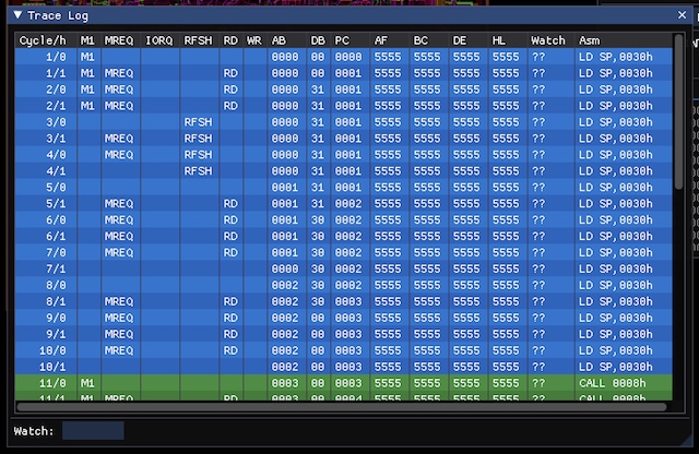
Opcode Fetch Machine Cycles
An Opcode Fetch looks like this in the tracelog (with all the relevant CPU state visible):
OPCODE FETCH:
┌─────┬────┬──────┬──────┬────┬──────┬────┬──────┬────┬────┬────┐
│  T  │ M1 │ MREQ │ RFSH │ RD │ AB   │ DB │ PC   │ IR │ I  │ R  │
├─────┼────┼──────┼──────┼────┼──────┼────┼──────┼────┼────┼────┤
│ 1/0 │ M1 │      │      │    │ 0004 │ 47 │ 0004 │ 47 │ 22 │ 03 │
│ 1/1 │ M1 │ MREQ │      │ RD │ 0004 │ 47 │ 0005 │ 47 │ 22 │ 03 │
│ 2/0 │ M1 │ MREQ │      │ RD │ 0004 │ 00 │ 0005 │ 47 │ 22 │ 03 │
│ 2/1 │ M1 │ MREQ │      │ RD │ 0004 │ 00 │ 0005 │ 00 │ 22 │ 03 │
│ 3/0 │    │      │ RFSH │    │ 2203 │ 00 │ 0005 │ 00 │ 22 │ 03 │
│ 3/1 │    │ MREQ │ RFSH │    │ 2203 │ 00 │ 0005 │ 00 │ 22 │ 04 │
│ 4/0 │    │ MREQ │ RFSH │    │ 2203 │ 00 │ 0005 │ 00 │ 22 │ 04 │
│ 4/1 │    │      │ RFSH │    │ 2200 │ 00 │ 0005 │ 00 │ 22 │ 04 │
Keep in mind that this shows half-clock-cycles, a 4-clock-cycle opcode-fetch machine cycle is shown as 8 half-clock-cycles in the trace log.
The M1, MREQ, RFSH and RD columns show the current state of the respective CPU pins.
AB and DB are “address bus” and “data bus”. IR is an internal register which holds the current opcode byte. I and R are the respective CPU registers (I is the upper byte of the interrupt vector, R is the ‘refresh counter’ register).
Let’s go through each half-cycle of an opcode-fetch machine cycle:
┌─────┬────┬──────┬──────┬────┬──────┬────┬──────┬────┬────┬────┐
│  T  │ M1 │ MREQ │ RFSH │ RD │ AB   │ DB │ PC   │ IR │ I  │ R  │
├─────┼────┼──────┼──────┼────┼──────┼────┼──────┼────┼────┼────┤
│ 1/0 │ M1 │      │      │    │ 0004 │ 47 │ 0004 │ 47 │ 22 │ 03 │
The M1 pin is set to active, and the address bus has been loaded with the current program counter (PC). The data bus and instruction register still have their values from the last instruction (which happened to an LD I,A instruction (byte sequence: ED 47).
┌─────┬────┬──────┬──────┬────┬──────┬────┬──────┬────┬────┬────┐
│  T  │ M1 │ MREQ │ RFSH │ RD │ AB   │ DB │ PC   │ IR │ I  │ R  │
├─────┼────┼──────┼──────┼────┼──────┼────┼──────┼────┼────┼────┤
│ 1/1 │ M1 │ MREQ │      │ RD │ 0004 │ 47 │ 0005 │ 47 │ 22 │ 03 │
In the next half cycle, the MREQ and RD pins have been set in addition to M1, which initiates a memory read from the address that’s currently on the address bus (0004). The program counter has been incremented to the next address.
┌─────┬────┬──────┬──────┬────┬──────┬────┬──────┬────┬────┬────┐
│  T  │ M1 │ MREQ │ RFSH │ RD │ AB   │ DB │ PC   │ IR │ I  │ R  │
├─────┼────┼──────┼──────┼────┼──────┼────┼──────┼────┼────┼────┤
│ 2/0 │ M1 │ MREQ │      │ RD │ 0004 │ 00 │ 0005 │ 47 │ 22 │ 03 │
Now the memory system has responded to the MREQ|RD pins being active by putting the content of address 0004 onto the data bus, which happens to be 00 (which is a NOP instruction). The instruction register hasn’t been updated yet.
┌─────┬────┬──────┬──────┬────┬──────┬────┬──────┬────┬────┬────┐
│  T  │ M1 │ MREQ │ RFSH │ RD │ AB   │ DB │ PC   │ IR │ I  │ R  │
├─────┼────┼──────┼──────┼────┼──────┼────┼──────┼────┼────┼────┤
│ 2/1 │ M1 │ MREQ │      │ RD │ 0004 │ 00 │ 0005 │ 00 │ 22 │ 03 │
In the next half cycle the 00 value on the data bus has been written into the instruction register (IR). This concludes the first half of the opcode fetch machine cycle.
┌─────┬────┬──────┬──────┬────┬──────┬────┬──────┬────┬────┬────┐
│  T  │ M1 │ MREQ │ RFSH │ RD │ AB   │ DB │ PC   │ IR │ I  │ R  │
├─────┼────┼──────┼──────┼────┼──────┼────┼──────┼────┼────┼────┤
│ 3/0 │    │      │ RFSH │    │ 2203 │ 00 │ 0005 │ 00 │ 22 │ 03 │
│ 3/1 │    │ MREQ │ RFSH │    │ 2203 │ 00 │ 0005 │ 00 │ 22 │ 04 │
│ 4/0 │    │ MREQ │ RFSH │    │ 2203 │ 00 │ 0005 │ 00 │ 22 │ 04 │
│ 4/1 │    │      │ RFSH │    │ 2200 │ 00 │ 0005 │ 00 │ 22 │ 04 │
The remaining 4 half-cycles (2 clock cycles) are spent with the Z80-specific ‘memory refresh’. A 16-bit value made from the registers I and R is put on the address bus, the M1 pin is set to inactive, the MREQ|RFSH pins to active and the R register is incremented. I haven’t figured out so far why the lower 8 bits on the address bus are cleared in the very last half-clock-cycle (this also happens in the last half-cycle of some other instructions).
Let’s quickly go over the remaining machine cycle types for completeness:
Memory Read Machine Cycles
A memory read machine cycle looks like this (in this case to load the byte value 22 from address 0001 into the register L):
MEM READ:
┌─────┬──────┬────┬──────┬────┬──────┐
│  T  │ MREQ │ RD │ AB   │ DB │ HL   │
├─────┼──────┼────┼──────┼────┼──────┤
│ 1/0 │      │    │ 0001 │ 21 │ 5555 │ <== address 0001 on address bus
│ 1/1 │ MREQ │ RD │ 0001 │ 21 │ 5555 │ <== MREQ|RD active
│ 2/0 │ MREQ │ RD │ 0001 │ 22 │ 5555 │ <== memory content 22 on data bus
│ 2/1 │ MREQ │ RD │ 0001 │ 22 │ 5555 │
│ 3/0 │ MREQ │ RD │ 0001 │ 22 │ 5555 │
│ 3/1 │      │    │ 0000 │ 22 │ 5522 │ <== target register L updated
Memory Write Machine Cycles
Here’s a memory write machine cycle to store the value in register A (33) into the address in register HL (1122):
MEM WRITE:
┌─────┬──────┬────┬──────┬────┬──────┬──────┐
│  T  │ MREQ │ WR │ AB   │ DB │ AF   │ HL   │
├─────┼──────┼────┼──────┼────┼──────┼──────┤
│ 1/0 │      │    │ 1122 │ 77 │ 3355 │ 1122 │ <== address 1122 on address bus
│ 1/1 │ MREQ │    │ 1122 │ 33 │ 3355 │ 1122 │ <== value 33 on data bus
│ 2/0 │ MREQ │    │ 1122 │ 33 │ 3355 │ 1122 │
│ 2/1 │ MREQ │ WR │ 1122 │ 33 │ 3355 │ 1122 │ <== MREQ|WR active
│ 3/0 │ MREQ │ WR │ 1122 │ 33 │ 3355 │ 1122 │
│ 3/1 │      │    │ 1122 │ 33 │ 3355 │ 1122 │
Note how the MREQ pin, address and data bus already contain the required values in the second half cycle (T1/1), but the WR (write) pin is only set active in the 4th half cycle (T2/1).
IO Read and Write Machine Cycles
The IO read and write machine cycles look similar, but are one clock cycle longer, and setting the CPU pins is delayed by a half-clock-cycle.
IO READ:
┌─────┬──────┬────┬────┬──────┬────┐
│  T  │ IORQ │ RD │ WR │ AB   │ DB │
├─────┼──────┼────┼────┼──────┼────┤
│ 1/0 │      │    │    │ 1122 │ 78 │
│ 1/1 │      │    │    │ 1122 │ 78 │
│ 2/0 │ IORQ │ RD │    │ 1122 │ 33 │
│ 2/1 │ IORQ │ RD │    │ 1122 │ 33 │
│ 3/0 │ IORQ │ RD │    │ 1122 │ 33 │
│ 3/1 │ IORQ │ RD │    │ 1122 │ 33 │
│ 4/0 │ IORQ │ RD │    │ 1122 │ 33 │
│ 4/1 │      │    │    │ 1122 │ 33 │
IO WRITE:
┌─────┬──────┬────┬────┬──────┬────┐
│  T  │ IORQ │ RD │ WR │ AB   │ DB │
├─────┼──────┼────┼────┼──────┼────┤
│ 1/0 │      │    │    │ 1122 │ 79 │
│ 1/1 │      │    │    │ 1122 │ 21 │
│ 2/0 │ IORQ │    │ WR │ 1122 │ 21 │
│ 2/1 │ IORQ │    │ WR │ 1122 │ 21 │
│ 3/0 │ IORQ │    │ WR │ 1122 │ 21 │
│ 3/1 │ IORQ │    │ WR │ 1122 │ 21 │
│ 4/0 │ IORQ │    │ WR │ 1122 │ 21 │
│ 4/1 │      │    │    │ 1122 │ 21 │
It’s interesting here that the ‘pin timing’ is identical between IO reads and writes. The WR pin is activated at the same moment as the IORQ pin, while in memory read machine cycles, the WR pin is activated two half cycles after the MREQ pin.
Wait states
All machine cycles that access memory or IO ports check the WAIT input pin at exactly one half-clock-cycle. If the WAIT pin is active, the execution ‘freezes’ until the WAIT pin goes inactive. The original intent was to give slow memory and IO devices time to react, but some computer systems also use wait states in more creative ways to arbitrate memory access between CPU and video hardware (for instance on the Amstrad CPC).
The exact (half-)clock cycle where the wait pin is sampled depends on the machine cycle type.
In the opcode fetch machine cycle, the wait pin is sampled in the second half-cycle of T2. If the WAIT pin isn’t active in this exact half-cycle, the CPU will not enter wait mode, otherwise the CPU will insert extra ‘wait cycles’ until the WAIT pin goes inactive.
For instance if the WAIT pin is only active in the second half cycle of T2, the opcode fetch machine cycle will be stretched from 4 to 5 clock cycles:
OPCODE FETCH:
┌─────┬────┬──────┬──────┬────┬────┬──────┬──────┬────┐
│  T  │ M1 │ MREQ │ RFSH │ RD │ WR │ WAIT │ AB   │ DB │
├─────┼────┼──────┼──────┼────┼────┼──────┼──────┼────┤
│ 1/0 │ M1 │      │      │    │    │      │ 0000 │ 00 │
│ 1/1 │ M1 │ MREQ │      │ RD │    │      │ 0000 │ 00 │
│ 2/0 │ M1 │ MREQ │      │ RD │    │      │ 0000 │ 31 │
│ 2/1 │ M1 │ MREQ │      │ RD │    │ WAIT │ 0000 │ 31 │ <== WAIT pin sampled here
│ 3/0 │ M1 │ MREQ │      │ RD │    │      │ 0000 │ 31 │ <== one extra clock cycle inserted
│ 3/1 │ M1 │ MREQ │      │ RD │    │      │ 0000 │ 31 │
│ 4/0 │    │      │ RFSH │    │    │      │ 0000 │ 31 │ <== regular execution continues here
│ 4/1 │    │ MREQ │ RFSH │    │    │      │ 0000 │ 31 │
│ 5/0 │    │ MREQ │ RFSH │    │    │      │ 0000 │ 31 │
│ 5/1 │    │      │ RFSH │    │    │      │ 0000 │ 31 │
If the wait pin goes inactive in the first half cycle, the CPU will leave the wait state mode at the end of the clock cycle:
OPCODE FETCH:
┌─────┬────┬──────┬──────┬────┬────┬──────┬──────┬────┐
│  T  │ M1 │ MREQ │ RFSH │ RD │ WR │ WAIT │ AB   │ DB │
├─────┼────┼──────┼──────┼────┼────┼──────┼──────┼────┤
│ 1/0 │ M1 │      │      │    │    │      │ 0000 │ 00 │
│ 1/1 │ M1 │ MREQ │      │ RD │    │      │ 0000 │ 00 │
│ 2/0 │ M1 │ MREQ │      │ RD │    │      │ 0000 │ 31 │
│ 2/1 │ M1 │ MREQ │      │ RD │    │ WAIT │ 0000 │ 31 │ <== WAIT pin sampled here
│ 3/0 │ M1 │ MREQ │      │ RD │    │ WAIT │ 0000 │ 31 │ <== WAIT pin active for 2 half cycles
│ 3/1 │ M1 │ MREQ │      │ RD │    │      │ 0000 │ 31 │ <== extra clock cycle completes
│ 4/0 │    │      │ RFSH │    │    │      │ 0000 │ 31 │ <== regular execution continues here
│ 4/1 │    │ MREQ │ RFSH │    │    │      │ 0000 │ 31 │
│ 5/0 │    │ MREQ │ RFSH │    │    │      │ 0000 │ 31 │
│ 5/1 │    │      │ RFSH │    │    │      │ 0000 │ 31 │
Setting the WAIT pin until the second half cycle causes one more clock cycle to be inserted:
OPCODE FETCH:
┌─────┬────┬──────┬──────┬────┬────┬──────┬──────┬────┐
│  T  │ M1 │ MREQ │ RFSH │ RD │ WR │ WAIT │ AB   │ DB │
├─────┼────┼──────┼──────┼────┼────┼──────┼──────┼────┤
│ 1/0 │ M1 │      │      │    │    │      │ 0000 │ 00 │
│ 1/1 │ M1 │ MREQ │      │ RD │    │      │ 0000 │ 00 │
│ 2/0 │ M1 │ MREQ │      │ RD │    │      │ 0000 │ 31 │
│ 2/1 │ M1 │ MREQ │      │ RD │    │ WAIT │ 0000 │ 31 │ <== WAIT pin sampled here
│ 3/0 │ M1 │ MREQ │      │ RD │    │ WAIT │ 0000 │ 31 │ <== WAIT pin active for 3 half cycles
│ 3/1 │ M1 │ MREQ │      │ RD │    │ WAIT │ 0000 │ 31 │ <== first inserted clock cycle completes
│ 4/0 │ M1 │ MREQ │      │ RD │    │      │ 0000 │ 31 │ <== a second wait clock cycle is inserted
│ 4/1 │ M1 │ MREQ │      │ RD │    │      │ 0000 │ 31 │
│ 5/0 │    │      │ RFSH │    │    │      │ 0000 │ 31 │ <== regular execution continues here
│ 5/1 │    │ MREQ │ RFSH │    │    │      │ 0000 │ 31 │
│ 6/0 │    │ MREQ │ RFSH │    │    │      │ 0000 │ 31 │
│ 6/1 │    │      │ RFSH │    │    │      │ 0000 │ 31 │
In memory-read machine-cycles, the WAIT pin is sampled at the second half cycle of T2 (same as in an opcode fetch).
MEM READ:
┌─────┬──────┬────┬────┬──────┬──────┬────┐
│  T  │ MREQ │ RD │ WR │ WAIT │ AB   │ DB │
├─────┼──────┼────┼────┼──────┼──────┼────┤
│ 1/0 │      │    │    │      │ 0001 │ 31 │
│ 1/1 │ MREQ │ RD │    │      │ 0001 │ 31 │
│ 2/0 │ MREQ │ RD │    │      │ 0001 │ 30 │
│ 2/1 │ MREQ │ RD │    │ WAIT │ 0001 │ 30 │ <== WAIT pin sampled here
│ 3/0 │ MREQ │ RD │    │      │ 0001 │ 30 │ <== extra clock cycle
│ 3/1 │ MREQ │ RD │    │      │ 0001 │ 30 │
│ 4/0 │ MREQ │ RD │    │      │ 0001 │ 30 │ <== regular execution continues
│ 4/1 │      │    │    │      │ 0000 │ 30 │
In memory write machine cycles, the WAIT pin is also sampled at the second half cycle of T2:
MEM WRITE:
┌─────┬──────┬────┬────┬──────┬──────┬────┐
│  T  │ MREQ │ RD │ WR │ WAIT │ AB   │ DB │
├─────┼──────┼────┼────┼──────┼──────┼────┤
│ 1/0 │      │    │    │      │ 1234 │ 77 │
│ 1/1 │ MREQ │    │    │      │ 1234 │ 11 │
│ 2/0 │ MREQ │    │    │      │ 1234 │ 11 │
│ 2/1 │ MREQ │    │ WR │ WAIT │ 1234 │ 11 │ <== WAIT pin sampled here
│ 3/0 │ MREQ │    │ WR │      │ 1234 │ 11 │ <== extra clock cycle
│ 3/1 │ MREQ │    │ WR │      │ 1234 │ 11 │
│ 4/0 │ MREQ │    │ WR │      │ 1234 │ 11 │ <== regular execution continues
│ 4/1 │      │    │    │      │ 1234 │ 11 │
In IO read and write machine cycles, the WAIT pin is sampled one full clock cycle later, at the second half-cycle of T3:
IO READ:
┌─────┬──────┬────┬────┬──────┬──────┬────┐
│  T  │ IORQ │ RD │ WR │ WAIT │ AB   │ DB │
├─────┼──────┼────┼────┼──────┼──────┼────┤
│ 1/0 │      │    │    │      │ 1234 │ 78 │
│ 1/1 │      │    │    │      │ 1234 │ 78 │
│ 2/0 │ IORQ │ RD │    │      │ 1234 │ FF │
│ 2/1 │ IORQ │ RD │    │      │ 1234 │ FF │
│ 3/0 │ IORQ │ RD │    │      │ 1234 │ FF │
│ 3/1 │ IORQ │ RD │    │ WAIT │ 1234 │ FF │ <== WAIT pin sampled here
│ 4/0 │ IORQ │ RD │    │      │ 1234 │ FF │ <== extra clock cycle
│ 4/1 │ IORQ │ RD │    │      │ 1234 │ FF │
│ 5/0 │ IORQ │ RD │    │      │ 1234 │ FF │ <== regular execution continues
│ 5/1 │      │    │    │      │ 1234 │ FF │
IO WRITE:
┌─────┬──────┬────┬────┬──────┬──────┬────┐
│  T  │ IORQ │ RD │ WR │ WAIT │ AB   │ DB │
├─────┼──────┼────┼────┼──────┼──────┼────┤
│ 1/0 │      │    │    │      │ 1234 │ 79 │
│ 1/1 │      │    │    │      │ 1234 │ 11 │
│ 2/0 │ IORQ │    │ WR │      │ 1234 │ 11 │
│ 2/1 │ IORQ │    │ WR │      │ 1234 │ 11 │
│ 3/0 │ IORQ │    │ WR │      │ 1234 │ 11 │
│ 3/1 │ IORQ │    │ WR │ WAIT │ 1234 │ 11 │ <== WAIT pin sampled here
│ 4/0 │ IORQ │    │ WR │      │ 1234 │ 11 │ <== extra clock cycle
│ 4/1 │ IORQ │    │ WR │      │ 1234 │ 11 │
│ 5/0 │ IORQ │    │ WR │      │ 1234 │ 11 │ <== regular execution continues
│ 5/1 │      │    │    │      │ 1234 │ 11 │
Extra Clock Cycles
With the knowledge that machine cycles are the basic building blocks of instructions, and the length of those machine cycles we should be able to predict the number of clock cycles in an instruction.
For instance LD HL,nnnn (load 16-bit immediate value into register pair HL) consists of the following machine cycles
- opcode fetch (4 clock cycles) to read the opcode byte
- a memory read (3 clock cycles) to read the next byte into L
- and another memory read (3 clock cycles) to read the next byte into H
Together: 4 + 3 + 3 = 10 clock cycles, which is totally correct.
The instruction PUSH HL (push content of HL register on the stack) should be the same, except that memory reads are replaced with memory writes:
- opcode fetch (4 clock cycles)
- a memory write to write H to the stack
- another memory write to write L to the stack
This should take 10 clock cycles too, but PUSH HL actually takes 11 clock cycles to execute:
PUSH HL:
┌─────┬────┬──────┬──────┬────┬────┬──────┬────┬──────┬──────┐
│  T  │ M1 │ MREQ │ RFSH │ RD │ WR │ AB   │ DB │ HL   │ SP   │
├─────┼────┼──────┼──────┼────┼────┼──────┼────┼──────┼──────┤
│ 1/0 │ M1 │      │      │    │    │ 0006 │ 12 │ 1234 │ 0100 │ <== opcode fetch
│ 1/1 │ M1 │ MREQ │      │ RD │    │ 0006 │ 12 │ 1234 │ 0100 │
│ 2/0 │ M1 │ MREQ │      │ RD │    │ 0006 │ E5 │ 1234 │ 0100 │
│ 2/1 │ M1 │ MREQ │      │ RD │    │ 0006 │ E5 │ 1234 │ 0100 │
│ 3/0 │    │      │ RFSH │    │    │ 0002 │ E5 │ 1234 │ 0100 │
│ 3/1 │    │ MREQ │ RFSH │    │    │ 0002 │ E5 │ 1234 │ 0100 │
│ 4/0 │    │ MREQ │ RFSH │    │    │ 0002 │ E5 │ 1234 │ 0100 │
│ 4/1 │    │      │ RFSH │    │    │ 0002 │ E5 │ 1234 │ 0100 │
│ 5/0 │    │      │      │    │    │ 0002 │ E5 │ 1234 │ 0100 │ <== WTF???
│ 5/1 │    │      │      │    │    │ 0000 │ E5 │ 1234 │ 00FF │ <== WTF???
│ 6/0 │    │      │      │    │    │ 00FF │ E5 │ 1234 │ 00FF │ <== memory write
│ 6/1 │    │ MREQ │      │    │    │ 00FF │ 12 │ 1234 │ 00FF │
│ 7/0 │    │ MREQ │      │    │    │ 00FF │ 12 │ 1234 │ 00FF │
│ 7/1 │    │ MREQ │      │    │ WR │ 00FF │ 12 │ 1234 │ 00FE │
│ 8/0 │    │ MREQ │      │    │ WR │ 00FF │ 12 │ 1234 │ 00FE │
│ 8/1 │    │      │      │    │    │ 00FE │ 12 │ 1234 │ 00FE │
│ 9/0 │    │      │      │    │    │ 00FE │ E5 │ 1234 │ 00FE │ <== memory write
│ 9/1 │    │ MREQ │      │    │    │ 00FE │ 34 │ 1234 │ 00FE │
│10/0 │    │ MREQ │      │    │    │ 00FE │ 34 │ 1234 │ 00FE │
│10/1 │    │ MREQ │      │    │ WR │ 00FE │ 34 │ 1234 │ 00FE │
│11/0 │    │ MREQ │      │    │ WR │ 00FE │ 34 │ 1234 │ 00FE │
│11/1 │    │      │      │    │    │ 00FE │ 34 │ 1234 │ 00FE │
There’s an additional clock cycle squeezed inbetween the opcode fetch and first memory read machine cycle which is used to ‘pre-decrement’ the SP register before the memory write machine cycles can happen.
It’s little irregularities like this which complicate writing a Z80 emulator. In a cycle correct emulator it is not only important that instructions take the correct number of clock cycles to execute, but also that memory and IO reads/writes happen at the correct clock cycle within the instruction.
Overlapped Execution
In some instructions, execution ‘leaks’ into the opcode fetch machine cycle of the next instruction.
For instance when inspecting the instruction ‘XOR A’ (which clears the A register and sets flags accordingly) the instruction doesn’t seem to have any effect:
XOR A:
┌─────┬────┬──────┬──────┬────┬────┬──────┬──────────┐
│  T  │ M1 │ MREQ │ RFSH │ RD │ WR │ AF   │ Flags    │
├─────┼────┼──────┼──────┼────┼────┼──────┼──────────┤
│ 1/0 │ M1 │      │      │    │    │ FFAC │ SzYhXVnc │
│ 1/1 │ M1 │ MREQ │      │ RD │    │ FFAC │ SzYhXVnc │
│ 2/0 │ M1 │ MREQ │      │ RD │    │ FFAC │ SzYhXVnc │
│ 2/1 │ M1 │ MREQ │      │ RD │    │ FFAC │ SzYhXVnc │
│ 3/0 │    │      │ RFSH │    │    │ FFAC │ SzYhXVnc │
│ 3/1 │    │ MREQ │ RFSH │    │    │ FFAC │ SzYhXVnc │
│ 4/0 │    │ MREQ │ RFSH │    │    │ FFAC │ SzYhXVnc │
│ 4/1 │    │      │ RFSH │    │    │ FFAC │ SzYhXVnc │ <== A and Flags not modified!
                                     ^^     ^^^^^^^^
XOR A takes 4 clock cycles, yet at the end of the instruction A isn’t zero, and the flag bits haven’t been updated either. Here’s the same diagram including the NOP instruction that follows:
XOR A + NOP:
┌─────┬────┬──────┬──────┬────┬────┬──────┬──────────┐
│  T  │ M1 │ MREQ │ RFSH │ RD │ WR │ AF   │ Flags    │
├─────┼────┼──────┼──────┼────┼────┼──────┼──────────┤
│ 1/0 │ M1 │      │      │    │    │ FFAC │ SzYhXVnc │ <== XOR A start
│ 1/1 │ M1 │ MREQ │      │ RD │    │ FFAC │ SzYhXVnc │
│ 2/0 │ M1 │ MREQ │      │ RD │    │ FFAC │ SzYhXVnc │
│ 2/1 │ M1 │ MREQ │      │ RD │    │ FFAC │ SzYhXVnc │
│ 3/0 │    │      │ RFSH │    │    │ FFAC │ SzYhXVnc │
│ 3/1 │    │ MREQ │ RFSH │    │    │ FFAC │ SzYhXVnc │
│ 4/0 │    │ MREQ │ RFSH │    │    │ FFAC │ SzYhXVnc │
│ 4/1 │    │      │ RFSH │    │    │ FFAC │ SzYhXVnc │
├─────┼────┼──────┼──────┼────┼────┼──────┼──────────┤
│ 1/0 │ M1 │      │      │    │    │ FFAC │ SzYhXVnc │ <== NOP starts here
│ 1/1 │ M1 │ MREQ │      │ RD │    │ FFAC │ SzYhXVnc │
│ 2/0 │ M1 │ MREQ │      │ RD │    │ FFAC │ SzYhXVnc │
│ 2/1 │ M1 │ MREQ │      │ RD │    │ 00AC │ SzYhXVnc │ <== A updated here
│ 3/0 │    │      │ RFSH │    │    │ 00AC │ SzYhXVnc │
│ 3/1 │    │ MREQ │ RFSH │    │    │ 0044 │ sZyhxVnc │ <== flags updated here
│ 4/0 │    │ MREQ │ RFSH │    │    │ 0044 │ sZyhxVnc │
│ 4/1 │    │      │ RFSH │    │    │ 0044 │ sZyhxVnc │
The results of the XOR A instruction only become available at the end of the second and third clock cycles of the following instruction.
Thankfully this overlapped execution is hardly relevant for CPU emulators, because it only affects the internal state of the CPU, not any state that’s observable from the outside.
The 3 Instruction Subsets
The Z80 instruction set is really 3 separate subsets each occupying 256 opcode ‘slots’. There’s the main instruction set which mostly overlaps with the Intel 8080 instruction set and two additional sets of instructions selected with the ED and CB prefix opcodes.
The main and CB subsets each occupy the full range of 256 instructions, while the ED subset is mostly empty and only implements 59 instructions.
I’m not counting the DD and FD prefix instruction ranges as separate subsets because they only slightly modify the behaviour of the main instructions.
This means there are 571 unique instructions in the Z80 instruction set (counting the RETI and RETN instructions as one because they have identical behaviour).
The 2-3-3 Opcode Bit Pattern
Opcode bytes can be split into three bit groups to reveal a hidden ‘octal structure’ of a 256 instruction subset:
  7 6   5 4 3   2 1 0
| x x | y y y | z z z |
The two top-most bits (xx) split the instruction space into 4 quadrants, and the remaining 6 bits are divided into two 3-bit groups (yyy) and (zzz) which are used as arguments to the instruction decoder.
Let’s look at each instruction subset and quadrant one by one:
Main Instructions
Main Quadrant 1 (xx = 01)
I’m starting with Main Quadrant 1 (not 0) because unlike 0 it is has a simple and ‘orderly’ structure. In an Z80 emulator this is usually the first quadrant I’m implementing.
The 64 instructions with the bit pattern |01|yyy|zzz| implement 8-bit move instructions where yyy defines the target and zzz the source. As a table, the main quadrant 1 looks like this:
| x=01 | z=000 | z=001 | z=010 | z=011 | z=100 | z=101 | z=110 | z=111 |
|---|---|---|---|---|---|---|---|---|
| y=000 | LD B,B | LD B,C | LD B,D | LD B,E | LD B,H | LD B,L | LD B,(HL) | LD B,A |
| y=001 | LD C,B | LD C,C | LD C,D | LD C,E | LD C,H | LD C,L | LD C,(HL) | LD C,A |
| y=010 | LD D,B | LD D,C | LD D,D | LD D,E | LD D,H | LD D,L | LD D,(HL) | LD D,A |
| y=011 | LD E,B | LD E,C | LD E,D | LD E,E | LD E,H | LD E,L | LD E,(HL) | LD E,A |
| y=100 | LD H,B | LD H,C | LD H,D | LD H,E | LD H,H | LD H,L | LD H,(HL) | LD H,A |
| y=101 | LD L,B | LD L,C | LD L,D | LD L,E | LD L,H | LD L,L | LD L,(HL) | LD L,A |
| y=110 | LD (HL),B | LD (HL),C | LD (HL),D | LD (HL),E | LD (HL),H | LD (HL),L | HALT | LD (HL),A |
| y=111 | LD A,B | LD A,C | LD A,D | LD A,E | LD A,H | LD A,L | LD A,(HL) | LD A,A |
I have choosen the green background for instructions that have no ‘timing surprises’ (like the PUSH HL instruction discussed above). The duration of ‘green’ instructions is simply the sum of their machine cycle default clock cycles. All instructions in the Main Quadrant 1 take 4 clock cycles (for the opcode fetch), except the instructions involving (HL) which take an additional memory read or write machine cycle, resulting in 7 clock cycles.
y and z are register indices as binary numbers:
000 = 0 => B
001 = 1 => C
010 = 2 => D
011 = 3 => E
100 = 4 => H
101 = 5 => L
110 = 6 => (HL)
111 = 7 => A
The ‘register index’ 6 is a bit special. According to the ‘hardware pattern’ of the Z80 register bank, index 6 would actually address the F (status flags) register, but this isn’t directly accessible in the instruction set (and ‘wasting’ one index for the F register in most instructions also wouldn’t make much sense). Instead index 6 is used as special case to load or store the 8-bit value in memory addressed by the register pair HL.
And another oddity is the HALT instruction at bit pattern |01|110|110| (== 76 hex). Following the ‘table logic’ this instruction slot should be occupied by an LD (HL),(HL) instruction which doesn’t make a lot of sense, so instead this slot was reused for the HALT instruction.
Main Quadrant 2 (xx = 10)
This is the second ‘beautiful’ quadrant in the main instruction set, this is where the basic 8-bit ALU instructions live:
| x=10 | z=000 | z=001 | z=010 | z=011 | z=100 | z=101 | z=110 | z=111 |
|---|---|---|---|---|---|---|---|---|
| y=000 | ADD B | ADD C | ADD D | ADD E | ADD H | ADD L | ADD (HL) | ADD A |
| y=001 | ADC B | ADC C | ADC D | ADC E | ADC H | ADC L | ADC (HL) | ADC A |
| y=010 | SUB B | SUB C | SUB D | SUB E | SUB H | SUB L | SUB (HL) | SUB A |
| y=011 | SBC B | SBC C | SBC D | SBC E | SBC H | SBC L | SBC (HL) | SBC A |
| y=100 | AND B | AND C | AND D | AND E | AND H | AND L | AND (HL) | AND A |
| y=101 | XOR B | XOR C | XOR D | XOR E | XOR H | XOR L | XOR (HL) | XOR A |
| y=110 | OR B | OR C | OR D | OR E | OR H | OR L | OR (HL) | OR A |
| y=111 | CP B | CP C | CP D | CP E | CP H | CP L | CP (HL) | CP A |
Again, no timing surprises in this quadrant. The z bit group selects the source register or (HL), and the y bit group the ALU operation:
000 => 0 => ADD
001 => 1 => ADC (add with carry)
010 => 2 => SUB
011 => 3 => SBC (sub with carry)
100 => 4 => AND
101 => 5 => XOR
110 => 6 => OR
111 => 7 => CP (compare - like SUB, but discard result)
This table also demonstrates nicely why all ALU operations implicitely use the register A to store the result. There’s simply no bits left in the 8-bit opcode to select a destination register.
Main Quadrant 0 (xx = 00)
This is the first of the two ‘messy’ quadrants in the main set:
| x=00 | z=000 | z=001 | z=010 | z=011 | z=100 | z=101 | z=110 | z=111 |
|---|---|---|---|---|---|---|---|---|
| y=000 | NOP | LD BC,nn | LD (BC),A | INC BC | INC B | DEC B | LD B,n | RLCA |
| y=001 | EX AF,AF' | ADD HL,BC | LD A,(BC) | DEC BC | INC C | DEC C | LD C,n | RRCA |
| y=010 | DJNZ d | LD DE,nn | LD (DE),A | INC DE | INC D | DEC D | LD D,n | RLA |
| y=011 | JR d | ADD HL,DE | LD A,(DE) | DEC DE | INC E | DEC E | LD E,n | RRA |
| y=100 | JR NZ,d | LD HL,nn | LD (nn),HL | INC HL | INC H | DEC H | LD H,n | DAA |
| y=101 | JR Z,d | ADD HL,HL | LD HL,(nn) | DEC HL | INC L | DEC L | LD L,n | CPL |
| y=110 | JR NC,d | LD SP,nn | LD (nn),A | INC SP | INC (HL) | DEC (HL) | LD (HL),n | SCF |
| y=111 | JR C,d | ADD HL,SP | LD A,(nn) | DEC SP | INC A | DEC A | LD A,n | CCF |
The red background color means that those instructions insert extra clock cycles between regular memory or IO machine cycles and need to be handled with special care in cycle-correct emulators. For the rest of the blog post I will focus on those ‘red’ instructions (because the timing of the ‘green’ instructions can trivially be derived from the instruction’s machine cycles).
INC/DEC (HL)
The INC (HL) and DEC (HL) instructions stick out, those are read-modify-write instructions. Let’s see why they have a red background:
INC (HL):
┌─────┬────┬──────┬──────┬────┬────┬──────┬────┐
│  T  │ M1 │ MREQ │ RFSH │ RD │ WR │ AB   │ DB │
├─────┼────┼──────┼──────┼────┼────┼──────┼────┤
│ 1/0 │ M1 │      │      │    │    │ 0003 │ 12 │ <== opcode fetch
│ 1/1 │ M1 │ MREQ │      │ RD │    │ 0003 │ 12 │
│ 2/0 │ M1 │ MREQ │      │ RD │    │ 0003 │ 34 │
│ 2/1 │ M1 │ MREQ │      │ RD │    │ 0000 │ 34 │
│ 3/0 │    │      │ RFSH │    │    │ 0001 │ 34 │
│ 3/1 │    │ MREQ │ RFSH │    │    │ 0001 │ 34 │
│ 4/0 │    │ MREQ │ RFSH │    │    │ 0001 │ 34 │
│ 4/1 │    │      │ RFSH │    │    │ 0000 │ 34 │
│ 5/0 │    │      │      │    │    │ 1234 │ 34 │ <== memory read
│ 5/1 │    │ MREQ │      │ RD │    │ 1234 │ 34 │
│ 6/0 │    │ MREQ │      │ RD │    │ 1234 │ 00 │
│ 6/1 │    │ MREQ │      │ RD │    │ 1234 │ 00 │
│ 7/0 │    │ MREQ │      │ RD │    │ 1234 │ 00 │
│ 7/1 │    │      │      │    │    │ 1234 │ 00 │
│ 8/0 │    │      │      │    │    │ 1234 │ 00 │ <== extra clock cycle
│ 8/1 │    │      │      │    │    │ 1234 │ 00 │
│ 9/0 │    │      │      │    │    │ 1234 │ 00 │ <== memory write
│ 9/1 │    │ MREQ │      │    │    │ 1234 │ 01 │
│10/0 │    │ MREQ │      │    │    │ 1234 │ 01 │
│10/1 │    │ MREQ │      │    │ WR │ 1234 │ 01 │
│11/0 │    │ MREQ │      │    │ WR │ 1234 │ 01 │
│11/1 │    │      │      │    │    │ 1234 │ 01 │
As expected, there’s an opcode fetch, memory read and memory write machine cycle. An extra clock cycle has been squeezed inbetween the read and write machine cycle, no doubt to increment the byte that’s been loaded from memory before it is written back.
INC/DEC ss
The 16-bit INC/DEC column adds two additional clock cycles after the opcode fetch machine cycle to perform the 16-bit math:
INC BC:
┌─────┬────┬──────┬──────┬────┬────┬──────┬────┬──────┐
│  T  │ M1 │ MREQ │ RFSH │ RD │ WR │ AB   │ DB │ BC   │
├─────┼────┼──────┼──────┼────┼────┼──────┼────┼──────┤
│ 1/0 │ M1 │      │      │    │    │ 0003 │ FF │ FFFF │ <== opcode fetch
│ 1/1 │ M1 │ MREQ │      │ RD │    │ 0003 │ FF │ FFFF │
│ 2/0 │ M1 │ MREQ │      │ RD │    │ 0003 │ 03 │ FFFF │
│ 2/1 │ M1 │ MREQ │      │ RD │    │ 0000 │ 03 │ FFFF │
│ 3/0 │    │      │ RFSH │    │    │ 0001 │ 03 │ FFFF │
│ 3/1 │    │ MREQ │ RFSH │    │    │ 0001 │ 03 │ FFFF │
│ 4/0 │    │ MREQ │ RFSH │    │    │ 0001 │ 03 │ FFFF │
│ 4/1 │    │      │ RFSH │    │    │ 0001 │ 03 │ FFFF │
│ 5/0 │    │      │      │    │    │ 0001 │ 03 │ FFFF │ <== 2 extra clock cycles
│ 5/1 │    │      │      │    │    │ 0001 │ 03 │ 0000 │
│ 6/0 │    │      │      │    │    │ 0001 │ 03 │ 0000 │
│ 6/1 │    │      │      │    │    │ 0000 │ 03 │ 0000 │
It’s interesting that the result is already available at the end of the first extra clock cycle. No idea why there’s a second ‘wasted’ clock cycle, especially since the 16-bit INC/DEC instructions don’t update the flag bits.
ADD HL,ss
The 16-bit ADD instructions add 7 extra clock cycles after the opcode fetch machine cycle:
ADD HL,DE
┌─────┬────┬──────┬──────┬────┬────┬──────┬────┬──────┬──────┐
│  T  │ M1 │ MREQ │ RFSH │ RD │ WR │ AB   │ DB │ DE   │ HL   │
├─────┼────┼──────┼──────┼────┼────┼──────┼────┼──────┼──────┤
│ 1/0 │ M1 │      │      │    │    │ 0006 │ 22 │ 2222 │ 1111 │ <== opcode fetch
│ 1/1 │ M1 │ MREQ │      │ RD │    │ 0006 │ 22 │ 2222 │ 1111 │
│ 2/0 │ M1 │ MREQ │      │ RD │    │ 0006 │ 19 │ 2222 │ 1111 │
│ 2/1 │ M1 │ MREQ │      │ RD │    │ 0006 │ 19 │ 2222 │ 1111 │
│ 3/0 │    │      │ RFSH │    │    │ 0002 │ 19 │ 2222 │ 1111 │
│ 3/1 │    │ MREQ │ RFSH │    │    │ 0002 │ 19 │ 2222 │ 1111 │
│ 4/0 │    │ MREQ │ RFSH │    │    │ 0002 │ 19 │ 2222 │ 1111 │
│ 4/1 │    │      │ RFSH │    │    │ 0002 │ 19 │ 2222 │ 1111 │
│ 5/0 │    │      │      │    │    │ 0002 │ 19 │ 2222 │ 1111 │ <== 7 extra clock cycles
│ 5/1 │    │      │      │    │    │ 0002 │ 19 │ 2222 │ 1111 │
│ 6/0 │    │      │      │    │    │ 0002 │ 19 │ 2222 │ 1111 │
│ 6/1 │    │      │      │    │    │ 0002 │ 19 │ 2222 │ 1111 │
│ 7/0 │    │      │      │    │    │ 0002 │ 19 │ 2222 │ 1111 │
│ 7/1 │    │      │      │    │    │ 0002 │ 19 │ 2222 │ 1133 │ <== result low byte
│ 8/0 │    │      │      │    │    │ 0002 │ 19 │ 2222 │ 1133 │
│ 8/1 │    │      │      │    │    │ 0002 │ 19 │ 2222 │ 1133 │
│ 9/0 │    │      │      │    │    │ 0002 │ 19 │ 2222 │ 1133 │
│ 9/1 │    │      │      │    │    │ 0002 │ 19 │ 2222 │ 1133 │
│10/0 │    │      │      │    │    │ 0002 │ 19 │ 2222 │ 1133 │
│10/1 │    │      │      │    │    │ 0002 │ 19 │ 2222 │ 1133 │
│11/0 │    │      │      │    │    │ 0002 │ 19 │ 2222 │ 1133 │
│11/1 │    │      │      │    │    │ 0002 │ 19 │ 2222 │ 3333 │ <== result high byte
This time, no clock cycles are wasted. The 16-bit result is only ready in the very last half cycle of the instruction. Not shown here is that the flag bits (H and C) are updated in the opcode fetch machine cycle of the next instruction (at M1/T3/1).
JR d
The relative jump JR d performs a regular memory read machine cycle after the opcode fetch, and then spends 5 more clock cycles to compute the jump target address:
JR d
┌─────┬────┬──────┬──────┬────┬────┬──────┬────┬──────┬──────┐
│  T  │ M1 │ MREQ │ RFSH │ RD │ WR │ AB   │ DB │ PC   │ WZ   │
├─────┼────┼──────┼──────┼────┼────┼──────┼────┼──────┼──────┤
│ 1/0 │ M1 │      │      │    │    │ 0002 │ 00 │ 0002 │ 5555 │ <== opcode fetch
│ 1/1 │ M1 │ MREQ │      │ RD │    │ 0002 │ 00 │ 0003 │ 5555 │
│ 2/0 │ M1 │ MREQ │      │ RD │    │ 0002 │ 18 │ 0003 │ 5555 │
│ 2/1 │ M1 │ MREQ │      │ RD │    │ 0002 │ 18 │ 0003 │ 5555 │
│ 3/0 │    │      │ RFSH │    │    │ 0002 │ 18 │ 0003 │ 5555 │
│ 3/1 │    │ MREQ │ RFSH │    │    │ 0002 │ 18 │ 0003 │ 5555 │
│ 4/0 │    │ MREQ │ RFSH │    │    │ 0002 │ 18 │ 0003 │ 5555 │
│ 4/1 │    │      │ RFSH │    │    │ 0002 │ 18 │ 0003 │ 5555 │
│ 5/0 │    │      │      │    │    │ 0003 │ 18 │ 0003 │ 5555 │ <== memory ready
│ 5/1 │    │ MREQ │      │ RD │    │ 0003 │ 18 │ 0004 │ 5555 │
│ 6/0 │    │ MREQ │      │ RD │    │ 0003 │ FC │ 0004 │ 5555 │
│ 6/1 │    │ MREQ │      │ RD │    │ 0003 │ FC │ 0004 │ 5555 │
│ 7/0 │    │ MREQ │      │ RD │    │ 0003 │ FC │ 0004 │ 5555 │
│ 7/1 │    │      │      │    │    │ 0003 │ FC │ 0004 │ 5555 │
│ 8/0 │    │      │      │    │    │ 0003 │ FC │ 0004 │ 5555 │ <== 5 extra clock cycles
│ 8/1 │    │      │      │    │    │ 0003 │ FC │ 0004 │ 5555 │
│ 9/0 │    │      │      │    │    │ 0003 │ FC │ 0004 │ 5555 │
│ 9/1 │    │      │      │    │    │ 0003 │ FC │ 0004 │ 5500 │
│10/0 │    │      │      │    │    │ 0003 │ FC │ 0004 │ 5500 │
│10/1 │    │      │      │    │    │ 0003 │ FC │ 0004 │ 5500 │
│11/0 │    │      │      │    │    │ 0003 │ FC │ 0004 │ 5500 │
│11/1 │    │      │      │    │    │ 0003 │ FC │ 0004 │ 5500 │
│12/0 │    │      │      │    │    │ 0003 │ FC │ 0004 │ 5500 │
│12/1 │    │      │      │    │    │ 0001 │ FC │ 0004 │ 0000 │ <== dst addr in WZ
The computed target address isn’t stored in the PC register, but instead in the internal 16-bit ‘helper’ register WZ. In fact the PC register never contains the actual target address (0000), it switches straight from the address following the JR d instruction (0004) to the address following the destination address:
JR d CONTINUED: NOP at the jump destination (address 0000)
┌─────┬────┬──────┬──────┬────┬────┬──────┬────┬──────┬──────┐
│  T  │ M1 │ MREQ │ RFSH │ RD │ WR │ AB   │ DB │ PC   │ WZ   │
├─────┼────┼──────┼──────┼────┼────┼──────┼────┼──────┼──────┤
│ 1/0 │ M1 │      │      │    │    │ 0000 │ FC │ 0004 │ 0000 │ <== PC still 0004!
│ 1/1 │ M1 │ MREQ │      │ RD │    │ 0000 │ FC │ 0001 │ 0000 │ <== PC goes right to 0001!
│ 2/0 │ M1 │ MREQ │      │ RD │    │ 0000 │ 00 │ 0001 │ 0000 │
│ 2/1 │ M1 │ MREQ │      │ RD │    │ 0000 │ 00 │ 0001 │ 0000 │
│ 3/0 │    │      │ RFSH │    │    │ 0003 │ 00 │ 0001 │ 0000 │
│ 3/1 │    │ MREQ │ RFSH │    │    │ 0003 │ 00 │ 0001 │ 0000 │
│ 4/0 │    │ MREQ │ RFSH │    │    │ 0003 │ 00 │ 0001 │ 0000 │
│ 4/1 │    │      │ RFSH │    │    │ 0000 │ 00 │ 0001 │ 0000 │
DJNZ d
The DJNZ d instruction (Decrement-and-Jump-if-Not-Zero) inserts one clock cycle between the opcode fetch and memory read machine cycle, and if the branch is taken, 5 additional clock cycles (this branch part is identical with the JR instruction):
DJNZ d - branch taken:
┌─────┬────┬──────┬──────┬────┬────┬──────┬────┬──────┬──────┬──────┐
│  T  │ M1 │ MREQ │ RFSH │ RD │ WR │ AB   │ DB │ PC   │ BC   │ WZ   │
├─────┼────┼──────┼──────┼────┼────┼──────┼────┼──────┼──────┼──────┤
│ 1/0 │ M1 │      │      │    │    │ 0003 │ 00 │ 0003 │ 0255 │ 5555 │ <== opcode fetch
│ 1/1 │ M1 │ MREQ │      │ RD │    │ 0003 │ 00 │ 0004 │ 0255 │ 5555 │
│ 2/0 │ M1 │ MREQ │      │ RD │    │ 0003 │ 10 │ 0004 │ 0255 │ 5555 │
│ 2/1 │ M1 │ MREQ │      │ RD │    │ 0000 │ 10 │ 0004 │ 0255 │ 5555 │
│ 3/0 │    │      │ RFSH │    │    │ 0002 │ 10 │ 0004 │ 0255 │ 5555 │
│ 3/1 │    │ MREQ │ RFSH │    │    │ 0002 │ 10 │ 0004 │ 0255 │ 5555 │
│ 4/0 │    │ MREQ │ RFSH │    │    │ 0002 │ 10 │ 0004 │ 0255 │ 5555 │
│ 4/1 │    │      │ RFSH │    │    │ 0002 │ 10 │ 0004 │ 0255 │ 5555 │
│ 5/0 │    │      │      │    │    │ 0002 │ 10 │ 0004 │ 0255 │ 5555 │ <== 1 extra clock cycle
│ 5/1 │    │      │      │    │    │ 0000 │ 10 │ 0004 │ 0255 │ 5555 │
│ 6/0 │    │      │      │    │    │ 0004 │ 10 │ 0004 │ 0255 │ 5555 │ <== memory read
│ 6/1 │    │ MREQ │      │ RD │    │ 0004 │ 10 │ 0005 │ 0155 │ 5555 │ <== B decremented
│ 7/0 │    │ MREQ │      │ RD │    │ 0004 │ FD │ 0005 │ 0155 │ 5555 │
│ 7/1 │    │ MREQ │      │ RD │    │ 0004 │ FD │ 0005 │ 0155 │ 5555 │
│ 8/0 │    │ MREQ │      │ RD │    │ 0004 │ FD │ 0005 │ 0155 │ 5555 │
│ 8/1 │    │      │      │    │    │ 0004 │ FD │ 0005 │ 0155 │ 5555 │
│ 9/0 │    │      │      │    │    │ 0004 │ FD │ 0005 │ 0155 │ 5555 │ <== 5 extra clock cycles
│ 9/1 │    │      │      │    │    │ 0004 │ FD │ 0005 │ 0155 │ 5555 │
│10/0 │    │      │      │    │    │ 0004 │ FD │ 0005 │ 0155 │ 5555 │
│10/1 │    │      │      │    │    │ 0004 │ FD │ 0005 │ 0155 │ 5502 │
│11/0 │    │      │      │    │    │ 0004 │ FD │ 0005 │ 0155 │ 5502 │
│11/1 │    │      │      │    │    │ 0004 │ FD │ 0005 │ 0155 │ 5502 │
│12/0 │    │      │      │    │    │ 0004 │ FD │ 0005 │ 0155 │ 5502 │
│12/1 │    │      │      │    │    │ 0004 │ FD │ 0005 │ 0155 │ 5502 │
│13/0 │    │      │      │    │    │ 0004 │ FD │ 0005 │ 0155 │ 5502 │
│13/1 │    │      │      │    │    │ 0004 │ FD │ 0005 │ 0155 │ 0002 │ <== dst addr in WZ
If the branch is not taken, DJNZ is finished right after the memory read:
DJNZ d - branch not taken:
┌─────┬────┬──────┬──────┬────┬────┬──────┬────┬──────┬──────┬──────┐
│  T  │ M1 │ MREQ │ RFSH │ RD │ WR │ AB   │ DB │ PC   │ BC   │ WZ   │
├─────┼────┼──────┼──────┼────┼────┼──────┼────┼──────┼──────┼──────┤
│ 1/0 │ M1 │      │      │    │    │ 0003 │ 00 │ 0003 │ 0155 │ 0002 │ <== opcode fetch
│ 1/1 │ M1 │ MREQ │      │ RD │    │ 0003 │ 00 │ 0004 │ 0155 │ 0002 │
│ 2/0 │ M1 │ MREQ │      │ RD │    │ 0003 │ 10 │ 0004 │ 0155 │ 0002 │
│ 2/1 │ M1 │ MREQ │      │ RD │    │ 0000 │ 10 │ 0004 │ 0155 │ 0002 │
│ 3/0 │    │      │ RFSH │    │    │ 0004 │ 10 │ 0004 │ 0155 │ 0002 │
│ 3/1 │    │ MREQ │ RFSH │    │    │ 0004 │ 10 │ 0004 │ 0155 │ 0002 │
│ 4/0 │    │ MREQ │ RFSH │    │    │ 0004 │ 10 │ 0004 │ 0155 │ 0002 │
│ 4/1 │    │      │ RFSH │    │    │ 0004 │ 10 │ 0004 │ 0155 │ 0002 │
│ 5/0 │    │      │      │    │    │ 0004 │ 10 │ 0004 │ 0155 │ 0002 │ <== 1 extra clock cycle
│ 5/1 │    │      │      │    │    │ 0004 │ 10 │ 0004 │ 0155 │ 0002 │
│ 6/0 │    │      │      │    │    │ 0004 │ 10 │ 0004 │ 0155 │ 0002 │ <== memory read
│ 6/1 │    │ MREQ │      │ RD │    │ 0004 │ 10 │ 0005 │ 0055 │ 0002 │ <== B decremented
│ 7/0 │    │ MREQ │      │ RD │    │ 0004 │ FD │ 0005 │ 0055 │ 0002 │
│ 7/1 │    │ MREQ │      │ RD │    │ 0004 │ FD │ 0005 │ 0055 │ 0002 │
│ 8/0 │    │ MREQ │      │ RD │    │ 0004 │ FD │ 0005 │ 0055 │ 0002 │
│ 8/1 │    │      │      │    │    │ 0004 │ FD │ 0005 │ 0055 │ 0002 │
JR cc,d
In the conditional relative jump instruction JR cc,d, the memory read directly follows the opcode fetch. If the branch is taken, 5 clock cycles are added, otherwise the instruction ends with the memory read machine cycle (so the branch behaviour is identical with DJNZ and JR):
JR cc,d - branch taken
┌─────┬────┬──────┬──────┬────┬────┬──────┬────┬──────┬──────┐
│  T  │ M1 │ MREQ │ RFSH │ RD │ WR │ AB   │ DB │ PC   │ WZ   │
├─────┼────┼──────┼──────┼────┼────┼──────┼────┼──────┼──────┤
│ 1/0 │ M1 │      │      │    │    │ 0003 │ 05 │ 0003 │ 5555 │ <== opcode fetch
│ 1/1 │ M1 │ MREQ │      │ RD │    │ 0003 │ 05 │ 0004 │ 5555 │
│ 2/0 │ M1 │ MREQ │      │ RD │    │ 0003 │ 20 │ 0004 │ 5555 │
│ 2/1 │ M1 │ MREQ │      │ RD │    │ 0000 │ 20 │ 0004 │ 5555 │
│ 3/0 │    │      │ RFSH │    │    │ 0002 │ 20 │ 0004 │ 5555 │
│ 3/1 │    │ MREQ │ RFSH │    │    │ 0002 │ 20 │ 0004 │ 5555 │
│ 4/0 │    │ MREQ │ RFSH │    │    │ 0002 │ 20 │ 0004 │ 5555 │
│ 4/1 │    │      │ RFSH │    │    │ 0002 │ 20 │ 0004 │ 5555 │
│ 5/0 │    │      │      │    │    │ 0004 │ 20 │ 0004 │ 5555 │ <== memory read
│ 5/1 │    │ MREQ │      │ RD │    │ 0004 │ 20 │ 0005 │ 5555 │
│ 6/0 │    │ MREQ │      │ RD │    │ 0004 │ FD │ 0005 │ 5555 │
│ 6/1 │    │ MREQ │      │ RD │    │ 0004 │ FD │ 0005 │ 5555 │
│ 7/0 │    │ MREQ │      │ RD │    │ 0004 │ FD │ 0005 │ 5555 │
│ 7/1 │    │      │      │    │    │ 0004 │ FD │ 0005 │ 5555 │
│ 8/0 │    │      │      │    │    │ 0004 │ FD │ 0005 │ 5555 │ <== 5 extra clock cycles
│ 8/1 │    │      │      │    │    │ 0004 │ FD │ 0005 │ 5555 │
│ 9/0 │    │      │      │    │    │ 0004 │ FD │ 0005 │ 5555 │
│ 9/1 │    │      │      │    │    │ 0004 │ FD │ 0005 │ 5502 │
│10/0 │    │      │      │    │    │ 0004 │ FD │ 0005 │ 5502 │
│10/1 │    │      │      │    │    │ 0004 │ FD │ 0005 │ 5502 │
│11/0 │    │      │      │    │    │ 0004 │ FD │ 0005 │ 5502 │
│11/1 │    │      │      │    │    │ 0004 │ FD │ 0005 │ 5502 │
│12/0 │    │      │      │    │    │ 0004 │ FD │ 0005 │ 5502 │
│12/1 │    │      │      │    │    │ 0004 │ FD │ 0005 │ 0002 │ <== dest addr in WZ
JR cc,d - branch not taken
┌─────┬────┬──────┬──────┬────┬────┬──────┬────┬──────┬──────┐
│  T  │ M1 │ MREQ │ RFSH │ RD │ WR │ AB   │ DB │ PC   │ WZ   │
├─────┼────┼──────┼──────┼────┼────┼──────┼────┼──────┼──────┤
│ 1/0 │ M1 │      │      │    │    │ 0003 │ 05 │ 0003 │ 5555 │ <== opcode fetch
│ 1/1 │ M1 │ MREQ │      │ RD │    │ 0003 │ 05 │ 0004 │ 5555 │
│ 2/0 │ M1 │ MREQ │      │ RD │    │ 0003 │ 20 │ 0004 │ 5555 │
│ 2/1 │ M1 │ MREQ │      │ RD │    │ 0000 │ 20 │ 0004 │ 5555 │
│ 3/0 │    │      │ RFSH │    │    │ 0002 │ 20 │ 0004 │ 5555 │
│ 3/1 │    │ MREQ │ RFSH │    │    │ 0002 │ 20 │ 0004 │ 5555 │
│ 4/0 │    │ MREQ │ RFSH │    │    │ 0002 │ 20 │ 0004 │ 5555 │
│ 4/1 │    │      │ RFSH │    │    │ 0002 │ 20 │ 0004 │ 5555 │
│ 5/0 │    │      │      │    │    │ 0004 │ 20 │ 0004 │ 5555 │ <== memory read
│ 5/1 │    │ MREQ │      │ RD │    │ 0004 │ 20 │ 0005 │ 5555 │
│ 6/0 │    │ MREQ │      │ RD │    │ 0004 │ FD │ 0005 │ 5555 │
│ 6/1 │    │ MREQ │      │ RD │    │ 0004 │ FD │ 0005 │ 5555 │
│ 7/0 │    │ MREQ │      │ RD │    │ 0004 │ FD │ 0005 │ 5555 │
│ 7/1 │    │      │      │    │    │ 0004 │ FD │ 0005 │ 5555 │
Main Quadrant 3 (xx == 11)
| x=11 | z=000 | z=001 | z=010 | z=011 | z=100 | z=101 | z=110 | z=111 |
|---|---|---|---|---|---|---|---|---|
| y=000 | RET NZ | POP BC | JP NZ,nn | JP nn | CALL NZ,nn | PUSH BC | ADD n | RST 0h |
| y=001 | RET Z | RET | JP Z,nn | CB prefix | CALL Z,nn | CALL nn | ADC n | RST 8h |
| y=010 | RET NC | POP DE | JP NC,nn | OUT (n),A | CALL NC,nn | PUSH DE | SUB n | RST 10h |
| y=011 | RET C | EXX | JP C,nn | IN A,(n) | CALL C,nn | DD prefix | SBC n | RST 18h |
| y=100 | RET PO | POP HL | JP PO,nn | EX (SP),HL | CALL PO,nn | PUSH HL | AND n | RST 20h |
| y=101 | RET PE | JP HL | JP PE,nn | EX DE,HL | CALL PE,nn | ED prefix | XOR n | RST 28h |
| y=110 | RET P | POP AF | JP P,nn | DI | CALL P,nn | PUSH AF | OR n | RST 30h |
| y=111 | RET M | LD SP,HL | JP M,nn | EI | CALL M,nn | FD prefix | CP n | RST 38h |
CALL nn
The CALL nn instruction inserts one clock cycle between the last memory read machine cycle (to load the destination address) and the first memory write machine cycle (to store the return address on the stack). The destination address is stored in WZ:
CALL nn
┌─────┬────┬──────┬──────┬────┬────┬──────┬────┬──────┬──────┬──────┐
│  T  │ M1 │ MREQ │ RFSH │ RD │ WR │ AB   │ DB │ PC   │ SP   │ WZ   │
├─────┼────┼──────┼──────┼────┼────┼──────┼────┼──────┼──────┼──────┤
│ 1/0 │ M1 │      │      │    │    │ 0000 │ 00 │ 0000 │ 0100 │ 5555 │ <== opcode fetch
│ 1/1 │ M1 │ MREQ │      │ RD │    │ 0000 │ 00 │ 0001 │ 0100 │ 5555 │
│ 2/0 │ M1 │ MREQ │      │ RD │    │ 0000 │ CD │ 0001 │ 0100 │ 5555 │
│ 2/1 │ M1 │ MREQ │      │ RD │    │ 0000 │ CD │ 0001 │ 0100 │ 5555 │
│ 3/0 │    │      │ RFSH │    │    │ 0000 │ CD │ 0001 │ 0100 │ 5555 │
│ 3/1 │    │ MREQ │ RFSH │    │    │ 0000 │ CD │ 0001 │ 0100 │ 5555 │
│ 4/0 │    │ MREQ │ RFSH │    │    │ 0000 │ CD │ 0001 │ 0100 │ 5555 │
│ 4/1 │    │      │ RFSH │    │    │ 0000 │ CD │ 0001 │ 0100 │ 5555 │
│ 5/0 │    │      │      │    │    │ 0001 │ CD │ 0001 │ 0100 │ 5555 │ <== memory read
│ 5/1 │    │ MREQ │      │ RD │    │ 0001 │ CD │ 0002 │ 0100 │ 5555 │
│ 6/0 │    │ MREQ │      │ RD │    │ 0001 │ 22 │ 0002 │ 0100 │ 5555 │
│ 6/1 │    │ MREQ │      │ RD │    │ 0001 │ 22 │ 0002 │ 0100 │ 5555 │
│ 7/0 │    │ MREQ │      │ RD │    │ 0001 │ 22 │ 0002 │ 0100 │ 5555 │
│ 7/1 │    │      │      │    │    │ 0000 │ 22 │ 0002 │ 0100 │ 5522 │
│ 8/0 │    │      │      │    │    │ 0002 │ 22 │ 0002 │ 0100 │ 5522 │ <== memory read
│ 8/1 │    │ MREQ │      │ RD │    │ 0002 │ 22 │ 0003 │ 0100 │ 5522 │
│ 9/0 │    │ MREQ │      │ RD │    │ 0002 │ 11 │ 0003 │ 0100 │ 5522 │
│ 9/1 │    │ MREQ │      │ RD │    │ 0002 │ 11 │ 0003 │ 0100 │ 5522 │
│10/0 │    │ MREQ │      │ RD │    │ 0002 │ 11 │ 0003 │ 0100 │ 5522 │
│10/1 │    │      │      │    │    │ 0002 │ 11 │ 0003 │ 0100 │ 1122 │ <== branch target in WZ
│11/0 │    │      │      │    │    │ 0002 │ 11 │ 0003 │ 0100 │ 1122 │ <== extra clock cycle
│11/1 │    │      │      │    │    │ 0000 │ 11 │ 0003 │ 00FF │ 1122 │ <== SP pre-decremented
│12/0 │    │      │      │    │    │ 5554 │ 11 │ 0003 │ 00FF │ 1122 │ <== memory write
│12/1 │    │ MREQ │      │    │    │ 5554 │ 00 │ 0003 │ 00FF │ 1122 │
│13/0 │    │ MREQ │      │    │    │ 5554 │ 00 │ 0003 │ 00FF │ 1122 │
│13/1 │    │ MREQ │      │    │ WR │ 5554 │ 00 │ 0003 │ 00FE │ 1122 │
│14/0 │    │ MREQ │      │    │ WR │ 5554 │ 00 │ 0003 │ 00FE │ 1122 │
│14/1 │    │      │      │    │    │ 5550 │ 00 │ 0003 │ 00FE │ 1122 │
│15/0 │    │      │      │    │    │ 5553 │ 11 │ 0003 │ 00FE │ 1122 │ <== memory write
│15/1 │    │ MREQ │      │    │    │ 5553 │ 03 │ 0003 │ 00FE │ 1122 │
│16/0 │    │ MREQ │      │    │    │ 5553 │ 03 │ 0003 │ 00FE │ 1122 │
│16/1 │    │ MREQ │      │    │ WR │ 5553 │ 03 │ 0003 │ 00FE │ 1122 │
│17/0 │    │ MREQ │      │    │ WR │ 5553 │ 03 │ 0003 │ 00FE │ 1122 │
│17/1 │    │      │      │    │    │ 5553 │ 03 │ 0003 │ 00FE │ 1122 │
Like in other branch instructions, the PC register isn’t updated in the instruction,
instead it switches to dst addr + 1 in the second half cycle of the first
subroutine instruction:
CALL nn - continued (first opcode fetch in subroutine)
┌─────┬────┬──────┬──────┬────┬────┬──────┬────┬──────┬──────┐
│  T  │ M1 │ MREQ │ RFSH │ RD │ WR │ AB   │ DB │ PC   │ WZ   │
├─────┼────┼──────┼──────┼────┼────┼──────┼────┼──────┼──────┤
│ 1/0 │ M1 │      │      │    │    │ 1122 │ 11 │ 0003 │ 1122 │ <== PC still at CALL nn + 1
│ 1/1 │ M1 │ MREQ │      │ RD │    │ 1122 │ 11 │ 1123 │ 1122 │ <== PC now at dst addr + 1
│ 2/0 │ M1 │ MREQ │      │ RD │    │ 1122 │ C9 │ 1123 │ 1122 │
│ 2/1 │ M1 │ MREQ │      │ RD │    │ 1122 │ C9 │ 1123 │ 1122 │
CALL cc,nn
The conditional CALL cc,nn instruction is exactly identical with the unconditional CALL nn instruction if the condition is true. Otherwise the instruction exits early after the second memory read:
CALL NZ,nn - branch not taken
┌─────┬────┬──────┬──────┬────┬────┬──────┬────┬──────┬──────┐
│  T  │ M1 │ MREQ │ RFSH │ RD │ WR │ AB   │ DB │ PC   │ WZ   │
├─────┼────┼──────┼──────┼────┼────┼──────┼────┼──────┼──────┤
│ 1/0 │ M1 │      │      │    │    │ 0003 │ 05 │ 0003 │ 5555 │ <== opcode fetch
│ 1/1 │ M1 │ MREQ │      │ RD │    │ 0003 │ 05 │ 0004 │ 5555 │
│ 2/0 │ M1 │ MREQ │      │ RD │    │ 0003 │ CC │ 0004 │ 5555 │
│ 2/1 │ M1 │ MREQ │      │ RD │    │ 0000 │ CC │ 0004 │ 5555 │
│ 3/0 │    │      │ RFSH │    │    │ 0002 │ CC │ 0004 │ 5555 │
│ 3/1 │    │ MREQ │ RFSH │    │    │ 0002 │ CC │ 0004 │ 5555 │
│ 4/0 │    │ MREQ │ RFSH │    │    │ 0002 │ CC │ 0004 │ 5555 │
│ 4/1 │    │      │ RFSH │    │    │ 0002 │ CC │ 0004 │ 5555 │
│ 5/0 │    │      │      │    │    │ 0004 │ CC │ 0004 │ 5555 │ <== memory read
│ 5/1 │    │ MREQ │      │ RD │    │ 0004 │ CC │ 0005 │ 5555 │
│ 6/0 │    │ MREQ │      │ RD │    │ 0004 │ 0B │ 0005 │ 5555 │
│ 6/1 │    │ MREQ │      │ RD │    │ 0004 │ 0B │ 0005 │ 5555 │
│ 7/0 │    │ MREQ │      │ RD │    │ 0004 │ 0B │ 0005 │ 5555 │
│ 7/1 │    │      │      │    │    │ 0004 │ 0B │ 0005 │ 550B │
│ 8/0 │    │      │      │    │    │ 0005 │ 0B │ 0005 │ 550B │ <== memory read
│ 8/1 │    │ MREQ │      │ RD │    │ 0005 │ 0B │ 0006 │ 550B │
│ 9/0 │    │ MREQ │      │ RD │    │ 0005 │ 00 │ 0006 │ 550B │
│ 9/1 │    │ MREQ │      │ RD │    │ 0005 │ 00 │ 0006 │ 550B │
│10/0 │    │ MREQ │      │ RD │    │ 0005 │ 00 │ 0006 │ 550B │
│10/1 │    │      │      │    │    │ 0005 │ 00 │ 0006 │ 000B │ <== dst addr in WZ
RET cc
The conditional return instructions RET cc adds or inserts one clock cycle after the opcode fetch. If the condition is false the instruction ends here, otherwise two more memory read machine cycles are added to load the return address from the stack into WZ.
RET Z - condition false
┌─────┬────┬──────┬──────┬────┬────┬──────┬────┬──────┬──────┬──────┐
│  T  │ M1 │ MREQ │ RFSH │ RD │ WR │ AB   │ DB │ PC   │ SP   │ WZ   │
├─────┼────┼──────┼──────┼────┼────┼──────┼────┼──────┼──────┼──────┤
│ 1/0 │ M1 │      │      │    │    │ 000C │ 05 │ 000C │ 00FE │ 0009 │ <== opcode fetch
│ 1/1 │ M1 │ MREQ │      │ RD │    │ 000C │ 05 │ 000D │ 00FE │ 0009 │
│ 2/0 │ M1 │ MREQ │      │ RD │    │ 000C │ C8 │ 000D │ 00FE │ 0009 │
│ 2/1 │ M1 │ MREQ │      │ RD │    │ 000C │ C8 │ 000D │ 00FE │ 0009 │
│ 3/0 │    │      │ RFSH │    │    │ 0004 │ C8 │ 000D │ 00FE │ 0009 │
│ 3/1 │    │ MREQ │ RFSH │    │    │ 0004 │ C8 │ 000D │ 00FE │ 0009 │
│ 4/0 │    │ MREQ │ RFSH │    │    │ 0004 │ C8 │ 000D │ 00FE │ 0009 │
│ 4/1 │    │      │ RFSH │    │    │ 0004 │ C8 │ 000D │ 00FE │ 0009 │
│ 5/0 │    │      │      │    │    │ 0004 │ C8 │ 000D │ 00FE │ 0009 │ <== one extra clock cycle
│ 5/1 │    │      │      │    │    │ 0004 │ C8 │ 000D │ 00FE │ 0009 │
RET Z - condition true
┌─────┬────┬──────┬──────┬────┬────┬──────┬────┬──────┬──────┬──────┐
│  T  │ M1 │ MREQ │ RFSH │ RD │ WR │ AB   │ DB │ PC   │ SP   │ WZ   │
├─────┼────┼──────┼──────┼────┼────┼──────┼────┼──────┼──────┼──────┤
│ 1/0 │ M1 │      │      │    │    │ 2005 │ 05 │ 2005 │ 00FE │ 2000 │ <== opcode fetch
│ 1/1 │ M1 │ MREQ │      │ RD │    │ 2005 │ 05 │ 2006 │ 00FE │ 2000 │
│ 2/0 │ M1 │ MREQ │      │ RD │    │ 2005 │ C8 │ 2006 │ 00FE │ 2000 │
│ 2/1 │ M1 │ MREQ │      │ RD │    │ 2004 │ C8 │ 2006 │ 00FE │ 2000 │
│ 3/0 │    │      │ RFSH │    │    │ 0006 │ C8 │ 2006 │ 00FE │ 2000 │
│ 3/1 │    │ MREQ │ RFSH │    │    │ 0006 │ C8 │ 2006 │ 00FE │ 2000 │
│ 4/0 │    │ MREQ │ RFSH │    │    │ 0006 │ C8 │ 2006 │ 00FE │ 2000 │
│ 4/1 │    │      │ RFSH │    │    │ 0006 │ C8 │ 2006 │ 00FE │ 2000 │
│ 5/0 │    │      │      │    │    │ 0006 │ C8 │ 2006 │ 00FE │ 2000 │ <== one extra clock cycle
│ 5/1 │    │      │      │    │    │ 0006 │ C8 │ 2006 │ 00FE │ 2000 │
│ 6/0 │    │      │      │    │    │ 00FE │ C8 │ 2006 │ 00FE │ 2000 │ <== memory read
│ 6/1 │    │ MREQ │      │ RD │    │ 00FE │ C8 │ 2006 │ 00FE │ 2000 │
│ 7/0 │    │ MREQ │      │ RD │    │ 00FE │ 06 │ 2006 │ 00FE │ 2000 │
│ 7/1 │    │ MREQ │      │ RD │    │ 00FE │ 06 │ 2006 │ 00FF │ 2000 │
│ 8/0 │    │ MREQ │      │ RD │    │ 00FE │ 06 │ 2006 │ 00FF │ 2000 │
│ 8/1 │    │      │      │    │    │ 00FE │ 06 │ 2006 │ 00FF │ 2006 │
│ 9/0 │    │      │      │    │    │ 00FF │ 06 │ 2006 │ 00FF │ 2006 │ <== memory read
│ 9/1 │    │ MREQ │      │ RD │    │ 00FF │ 06 │ 2006 │ 00FF │ 2006 │
│10/0 │    │ MREQ │      │ RD │    │ 00FF │ 00 │ 2006 │ 00FF │ 2006 │
│10/1 │    │ MREQ │      │ RD │    │ 00FF │ 00 │ 2006 │ 0100 │ 2006 │
│11/0 │    │ MREQ │      │ RD │    │ 00FF │ 00 │ 2006 │ 0100 │ 2006 │
│11/1 │    │      │      │    │    │ 0000 │ 00 │ 2006 │ 0100 │ 0006 │ <== ret addr in WZ
LD SP,HL
The LD SP,HL instruction just adds two clock cycles after the opcode fetch:
LD SP,HL
┌─────┬────┬──────┬──────┬────┬────┬──────┬────┬──────┬──────┬──────┐
│  T  │ M1 │ MREQ │ RFSH │ RD │ WR │ AB   │ DB │ PC   │ HL   │ SP   │
├─────┼────┼──────┼──────┼────┼────┼──────┼────┼──────┼──────┼──────┤
│ 1/0 │ M1 │      │      │    │    │ 0003 │ 11 │ 0003 │ 1122 │ 5555 │ <== opcode fetch
│ 1/1 │ M1 │ MREQ │      │ RD │    │ 0003 │ 11 │ 0004 │ 1122 │ 5555 │
│ 2/0 │ M1 │ MREQ │      │ RD │    │ 0003 │ F9 │ 0004 │ 1122 │ 5555 │
│ 2/1 │ M1 │ MREQ │      │ RD │    │ 0000 │ F9 │ 0004 │ 1122 │ 5555 │
│ 3/0 │    │      │ RFSH │    │    │ 0001 │ F9 │ 0004 │ 1122 │ 5555 │
│ 3/1 │    │ MREQ │ RFSH │    │    │ 0001 │ F9 │ 0004 │ 1122 │ 5555 │
│ 4/0 │    │ MREQ │ RFSH │    │    │ 0001 │ F9 │ 0004 │ 1122 │ 5555 │
│ 4/1 │    │      │ RFSH │    │    │ 0001 │ F9 │ 0004 │ 1122 │ 5555 │
│ 5/0 │    │      │      │    │    │ 0001 │ F9 │ 0004 │ 1122 │ 5555 │ <== 2 extra clock cycles
│ 5/1 │    │      │      │    │    │ 0001 │ F9 │ 0004 │ 1122 │ 1122 │
│ 6/0 │    │      │      │    │    │ 0001 │ F9 │ 0004 │ 1122 │ 1122 │
│ 6/1 │    │      │      │    │    │ 0000 │ F9 │ 0004 │ 1122 │ 1122 │
EX (SP),HL
The EX (SP),HL instruction inserts one clock cycle between the last memory read and first memory write machine cycle, and adds 2 more clock cycles after the last memory write. The WZ register is used as intermediate storage for the 16-bit value read from the stack:
EX (SP),HL
┌─────┬────┬──────┬──────┬────┬────┬──────┬────┬──────┬──────┬──────┬──────┐
│  T  │ M1 │ MREQ │ RFSH │ RD │ WR │ AB   │ DB │ PC   │ HL   │ SP   │ WZ   │
├─────┼────┼──────┼──────┼────┼────┼──────┼────┼──────┼──────┼──────┼──────┤
│ 1/0 │ M1 │      │      │    │    │ 000A │ D5 │ 000A │ 4321 │ 00FE │ 5555 │ <== opcode fetch
│ 1/1 │ M1 │ MREQ │      │ RD │    │ 000A │ D5 │ 000B │ 4321 │ 00FE │ 5555 │
│ 2/0 │ M1 │ MREQ │      │ RD │    │ 000A │ E3 │ 000B │ 4321 │ 00FE │ 5555 │
│ 2/1 │ M1 │ MREQ │      │ RD │    │ 000A │ E3 │ 000B │ 4321 │ 00FE │ 5555 │
│ 3/0 │    │      │ RFSH │    │    │ 0004 │ E3 │ 000B │ 4321 │ 00FE │ 5555 │
│ 3/1 │    │ MREQ │ RFSH │    │    │ 0004 │ E3 │ 000B │ 4321 │ 00FE │ 5555 │
│ 4/0 │    │ MREQ │ RFSH │    │    │ 0004 │ E3 │ 000B │ 4321 │ 00FE │ 5555 │
│ 4/1 │    │      │ RFSH │    │    │ 0004 │ E3 │ 000B │ 4321 │ 00FE │ 5555 │
│ 5/0 │    │      │      │    │    │ 00FE │ E3 │ 000B │ 4321 │ 00FE │ 5555 │ <== memory read
│ 5/1 │    │ MREQ │      │ RD │    │ 00FE │ E3 │ 000B │ 4321 │ 00FE │ 5555 │
│ 6/0 │    │ MREQ │      │ RD │    │ 00FE │ 34 │ 000B │ 4321 │ 00FE │ 5555 │
│ 6/1 │    │ MREQ │      │ RD │    │ 00FE │ 34 │ 000B │ 4321 │ 00FE │ 00FF │
│ 7/0 │    │ MREQ │      │ RD │    │ 00FE │ 34 │ 000B │ 4321 │ 00FE │ 00FF │
│ 7/1 │    │      │      │    │    │ 00FE │ 34 │ 000B │ 4321 │ 00FE │ 0034 │ <== Z: low byte from stack
│ 8/0 │    │      │      │    │    │ 00FF │ 34 │ 000B │ 4321 │ 00FE │ 0034 │ <== memory read
│ 8/1 │    │ MREQ │      │ RD │    │ 00FF │ 34 │ 000B │ 4321 │ 00FE │ 0034 │
│ 9/0 │    │ MREQ │      │ RD │    │ 00FF │ 12 │ 000B │ 4321 │ 00FE │ 0034 │
│ 9/1 │    │ MREQ │      │ RD │    │ 00FF │ 12 │ 000B │ 4321 │ 00FE │ 0034 │
│10/0 │    │ MREQ │      │ RD │    │ 00FF │ 12 │ 000B │ 4321 │ 00FE │ 0034 │
│10/1 │    │      │      │    │    │ 00FF │ 12 │ 000B │ 4321 │ 00FE │ 1234 │ <== WZ: 16 bit value from stack
│11/0 │    │      │      │    │    │ 00FF │ 12 │ 000B │ 4321 │ 00FE │ 1234 │ <== extra clock cycle
│11/1 │    │      │      │    │    │ 00FE │ 12 │ 000B │ 4321 │ 00FF │ 1234 │ <== SP incremented
│12/0 │    │      │      │    │    │ 00FF │ 12 │ 000B │ 4321 │ 00FF │ 1234 │ <== memory write (L => stack)
│12/1 │    │ MREQ │      │    │    │ 00FF │ 43 │ 000B │ 4321 │ 00FF │ 1234 │
│13/0 │    │ MREQ │      │    │    │ 00FF │ 43 │ 000B │ 4321 │ 00FF │ 1234 │
│13/1 │    │ MREQ │      │    │ WR │ 00FF │ 43 │ 000B │ 4321 │ 00FE │ 1234 │ <== SP decremented again
│14/0 │    │ MREQ │      │    │ WR │ 00FF │ 43 │ 000B │ 4321 │ 00FE │ 1234 │
│14/1 │    │      │      │    │    │ 00FE │ 43 │ 000B │ 4321 │ 00FE │ 1234 │
│15/0 │    │      │      │    │    │ 00FE │ 12 │ 000B │ 4321 │ 00FE │ 1234 │ <== memory write (H => stack)
│15/1 │    │ MREQ │      │    │    │ 00FE │ 21 │ 000B │ 4321 │ 00FE │ 1234 │
│16/0 │    │ MREQ │      │    │    │ 00FE │ 21 │ 000B │ 4321 │ 00FE │ 1234 │
│16/1 │    │ MREQ │      │    │ WR │ 00FE │ 21 │ 000B │ 4321 │ 00FE │ 1234 │
│17/0 │    │ MREQ │      │    │ WR │ 00FE │ 21 │ 000B │ 4321 │ 00FE │ 1234 │
│17/1 │    │      │      │    │    │ 00FE │ 21 │ 000B │ 4321 │ 00FE │ 1234 │
│18/0 │    │      │      │    │    │ 00FE │ 21 │ 000B │ 4321 │ 00FE │ 1234 │ <== two extra clock cycles
│18/1 │    │      │      │    │    │ 00FE │ 21 │ 000B │ 1234 │ 00FE │ 1234 │ <== WZ => HL
│19/0 │    │      │      │    │    │ 00FE │ 21 │ 000B │ 1234 │ 00FE │ 1234 │
│19/1 │    │      │      │    │    │ 0034 │ 21 │ 000B │ 1234 │ 00FE │ 1234 │
PUSH qq
The PUSH instruction inserts one clock cycle between the opcode fetch and first memory write machine cycle:
PUSH DE:
┌─────┬────┬──────┬──────┬────┬────┬──────┬────┬──────┬──────┬──────┐
│  T  │ M1 │ MREQ │ RFSH │ RD │ WR │ AB   │ DB │ PC   │ DE   │ SP   │
├─────┼────┼──────┼──────┼────┼────┼──────┼────┼──────┼──────┼──────┤
│ 1/0 │ M1 │      │      │    │    │ 0006 │ 12 │ 0006 │ 1234 │ 0100 │ <== opcode fetch
│ 1/1 │ M1 │ MREQ │      │ RD │    │ 0006 │ 12 │ 0007 │ 1234 │ 0100 │
│ 2/0 │ M1 │ MREQ │      │ RD │    │ 0006 │ D5 │ 0007 │ 1234 │ 0100 │
│ 2/1 │ M1 │ MREQ │      │ RD │    │ 0006 │ D5 │ 0007 │ 1234 │ 0100 │
│ 3/0 │    │      │ RFSH │    │    │ 0002 │ D5 │ 0007 │ 1234 │ 0100 │
│ 3/1 │    │ MREQ │ RFSH │    │    │ 0002 │ D5 │ 0007 │ 1234 │ 0100 │
│ 4/0 │    │ MREQ │ RFSH │    │    │ 0002 │ D5 │ 0007 │ 1234 │ 0100 │
│ 4/1 │    │      │ RFSH │    │    │ 0002 │ D5 │ 0007 │ 1234 │ 0100 │
│ 5/0 │    │      │      │    │    │ 0002 │ D5 │ 0007 │ 1234 │ 0100 │ <== extra clock cycle
│ 5/1 │    │      │      │    │    │ 0000 │ D5 │ 0007 │ 1234 │ 00FF │ <== SP pre-decremented
│ 6/0 │    │      │      │    │    │ 00FF │ D5 │ 0007 │ 1234 │ 00FF │ <== memory write
│ 6/1 │    │ MREQ │      │    │    │ 00FF │ 12 │ 0007 │ 1234 │ 00FF │
│ 7/0 │    │ MREQ │      │    │    │ 00FF │ 12 │ 0007 │ 1234 │ 00FF │
│ 7/1 │    │ MREQ │      │    │ WR │ 00FF │ 12 │ 0007 │ 1234 │ 00FE │
│ 8/0 │    │ MREQ │      │    │ WR │ 00FF │ 12 │ 0007 │ 1234 │ 00FE │
│ 8/1 │    │      │      │    │    │ 00FE │ 12 │ 0007 │ 1234 │ 00FE │
│ 9/0 │    │      │      │    │    │ 00FE │ D5 │ 0007 │ 1234 │ 00FE │ <== memory write
│ 9/1 │    │ MREQ │      │    │    │ 00FE │ 34 │ 0007 │ 1234 │ 00FE │
│10/0 │    │ MREQ │      │    │    │ 00FE │ 34 │ 0007 │ 1234 │ 00FE │
│10/1 │    │ MREQ │      │    │ WR │ 00FE │ 34 │ 0007 │ 1234 │ 00FE │
│11/0 │    │ MREQ │      │    │ WR │ 00FE │ 34 │ 0007 │ 1234 │ 00FE │
│11/1 │    │      │      │    │    │ 00FE │ 34 │ 0007 │ 1234 │ 00FE │
RST p
The RST p instructions insert one clock cycle between the opcode fetch and first memory write machine cycle to pre-decrement the stack pointer. The WZ register is used as temporary storage of the destination address:
RST 20h
┌─────┬────┬──────┬──────┬────┬────┬──────┬────┬──────┬──────┬──────┐
│  T  │ M1 │ MREQ │ RFSH │ RD │ WR │ AB   │ DB │ PC   │ SP   │ WZ   │
├─────┼────┼──────┼──────┼────┼────┼──────┼────┼──────┼──────┼──────┤
│ 1/0 │ M1 │      │      │    │    │ 0003 │ 01 │ 0003 │ 0100 │ 5555 │ <== opcode fetch
│ 1/1 │ M1 │ MREQ │      │ RD │    │ 0003 │ 01 │ 0004 │ 0100 │ 5555 │
│ 2/0 │ M1 │ MREQ │      │ RD │    │ 0003 │ E7 │ 0004 │ 0100 │ 5555 │
│ 2/1 │ M1 │ MREQ │      │ RD │    │ 0000 │ E7 │ 0004 │ 0100 │ 5555 │
│ 3/0 │    │      │ RFSH │    │    │ 0001 │ E7 │ 0004 │ 0100 │ 5555 │
│ 3/1 │    │ MREQ │ RFSH │    │    │ 0001 │ E7 │ 0004 │ 0100 │ 5555 │
│ 4/0 │    │ MREQ │ RFSH │    │    │ 0001 │ E7 │ 0004 │ 0100 │ 5555 │
│ 4/1 │    │      │ RFSH │    │    │ 0001 │ E7 │ 0004 │ 0100 │ 5555 │
│ 5/0 │    │      │      │    │    │ 0001 │ E7 │ 0004 │ 0100 │ 5555 │ <== extra clock cycle
│ 5/1 │    │      │      │    │    │ 0000 │ E7 │ 0004 │ 00FF │ 5555 │ <== SP pre-decremented
│ 6/0 │    │      │      │    │    │ 00FF │ E7 │ 0004 │ 00FF │ 5555 │ <== memory write
│ 6/1 │    │ MREQ │      │    │    │ 00FF │ 00 │ 0004 │ 00FF │ 5555 │
│ 7/0 │    │ MREQ │      │    │    │ 00FF │ 00 │ 0004 │ 00FF │ 5555 │
│ 7/1 │    │ MREQ │      │    │ WR │ 00FF │ 00 │ 0004 │ 00FE │ 5555 │
│ 8/0 │    │ MREQ │      │    │ WR │ 00FF │ 00 │ 0004 │ 00FE │ 5555 │
│ 8/1 │    │      │      │    │    │ 00FE │ 00 │ 0004 │ 00FE │ 5520 │
│ 9/0 │    │      │      │    │    │ 00FE │ E7 │ 0004 │ 00FE │ 5520 │ <== memory write
│ 9/1 │    │ MREQ │      │    │    │ 00FE │ 04 │ 0004 │ 00FE │ 5520 │
│10/0 │    │ MREQ │      │    │    │ 00FE │ 04 │ 0004 │ 00FE │ 5520 │
│10/1 │    │ MREQ │      │    │ WR │ 00FE │ 04 │ 0004 │ 00FE │ 5520 │
│11/0 │    │ MREQ │      │    │ WR │ 00FE │ 04 │ 0004 │ 00FE │ 5520 │
│11/1 │    │      │      │    │    │ 00FE │ 04 │ 0004 │ 00FE │ 0020 │ <== WZ dst addr
Like in other branch instructions, PC isn’t updated within the instruction, instead it switches from the address following the RST instruction to the destination address + 1 in the second half-cycle of the first subroutine opcode fetch:
RST 20h - continued into subroutine
┌─────┬────┬──────┬──────┬────┬────┬──────┬────┬──────┬──────┬──────┐
│  T  │ M1 │ MREQ │ RFSH │ RD │ WR │ AB   │ DB │ PC   │ SP   │ WZ   │
├─────┼────┼──────┼──────┼────┼────┼──────┼────┼──────┼──────┼──────┤
│ 1/0 │ M1 │      │      │    │    │ 0020 │ E7 │ 0004 │ 00FE │ 0020 │ <== opcode fetch, PC still at RST 20h + 1
│ 1/1 │ M1 │ MREQ │      │ RD │    │ 0020 │ E7 │ 0021 │ 00FE │ 0020 │ <== PC now at dst addr + 1
│ 2/0 │ M1 │ MREQ │      │ RD │    │ 0020 │ C9 │ 0021 │ 00FE │ 0020 │
│ 2/1 │ M1 │ MREQ │      │ RD │    │ 0020 │ C9 │ 0021 │ 00FE │ 0020 │
Prefix Instruction Overview
All prefix bytes (CB, DD, ED, FD) execute as regular 4-cycle instruction, except:
- no interrupts are handled at the end of the prefix instruction
- the decoding of the following opcode is modified:
- the ED and CB prefixes each select an entirely different instruction subset
- the DD and FD prefix select the main instruction subset but replace usage of HL with IX or IY (highly simplified, see the DD/FD section for details)
- the ED prefix cancels any “active effects” of the DD and FD prefixes (for instance the byte sequence DD ED B0 doesn’t cause the LDIR instruction to use IX instead of HL)
Sequences of the same prefix byte sometimes behave unexpected:
-
Sequences of DD or FD, or a mix of them inhibit interrupt handling until the end of the instruction following the DD/FD sequence. The following instruction will be modified depending on the last prefix byte in the sequence. DD and FD prefixes don’t ‘stack’, e.g. it’s not possible to load the 16-bit value 3333h into both IX and IY with the following byte sequence: DD FD 21 33 33, instead the FD prefix cancels the effect of the DD prefix, and only the IY register is loaded with the value.
-
Sequences of ED prefixes will be interpreted as pairs of ED ED opcode bytes (which simply acts as an 8-cycle NOP)
-
Sequences of CB prefixes will be interpreted as pairs of CB CB which is the regular SET 1,E instruction
-
DD/FD CB sequences result in the most weird behaviour and deserve their own section
The special ‘chaining behaviour’ of the DD and FD prefixes is simply a side effect of those prefixes not switching to a different instruction subset. If the next byte is a DD, ED, CB or FD, it will be execute as the respective prefix instruction.
DD and FD Prefixes
The DD and FD prefix instructions modify the behaviour of the following opcode byte as follows:
All uses of the L, H, HL and (HL) will be replaced with IXL, IXH, IX and (IX+d) (for the DD prefix), or IYL, IYH, IY and (IY+d) (for the FD prefix), with the following exceptions:
- If (HL) and L or H are used in the same instruction, L and H are not replaced with IXL or IXH, for instance LD L,(IX+d) stores the content of (IX+d) into L, not IXL.
- In the instruction EX DE,HL, HL will not be replaced with IX or IY.
Instructions which are reinterpreted from (HL) to (IX+d) or (IY+d) load an additional offset byte ‘d’ which is signed-added to IX or IY to form the effective address for the memory access. This extra work consists of a regular memory read machine cycle (3 clock cycles) followed by 5 extra clock cycles to compute the resulting address which will be stored in WZ:
LD A,(IX+3)
┌─────┬────┬──────┬──────┬────┬────┬──────┬────┬──────┬──────┬──────┐
│  T  │ M1 │ MREQ │ RFSH │ RD │ WR │ AB   │ DB │ PC   │ IX   │ WZ   │
├─────┼────┼──────┼──────┼────┼────┼──────┼────┼──────┼──────┼──────┤
│ 1/0 │ M1 │      │      │    │    │ 0004 │ 20 │ 0004 │ 2000 │ 5555 │ <== opcode fetch DD prefix
│ 1/1 │ M1 │ MREQ │      │ RD │    │ 0004 │ 20 │ 0005 │ 2000 │ 5555 │
│ 2/0 │ M1 │ MREQ │      │ RD │    │ 0004 │ DD │ 0005 │ 2000 │ 5555 │
│ 2/1 │ M1 │ MREQ │      │ RD │    │ 0004 │ DD │ 0005 │ 2000 │ 5555 │
│ 3/0 │    │      │ RFSH │    │    │ 0002 │ DD │ 0005 │ 2000 │ 5555 │
│ 3/1 │    │ MREQ │ RFSH │    │    │ 0002 │ DD │ 0005 │ 2000 │ 5555 │
│ 4/0 │    │ MREQ │ RFSH │    │    │ 0002 │ DD │ 0005 │ 2000 │ 5555 │
│ 4/1 │    │      │ RFSH │    │    │ 0002 │ DD │ 0005 │ 2000 │ 5555 │
│ 5/0 │ M1 │      │      │    │    │ 0005 │ DD │ 0005 │ 2000 │ 5555 │ <== ocode fetch LD A,(HL)
│ 5/1 │ M1 │ MREQ │      │ RD │    │ 0005 │ DD │ 0006 │ 2000 │ 5555 │
│ 6/0 │ M1 │ MREQ │      │ RD │    │ 0005 │ 7E │ 0006 │ 2000 │ 5555 │
│ 6/1 │ M1 │ MREQ │      │ RD │    │ 0004 │ 7E │ 0006 │ 2000 │ 5555 │
│ 7/0 │    │      │ RFSH │    │    │ 0003 │ 7E │ 0006 │ 2000 │ 5555 │
│ 7/1 │    │ MREQ │ RFSH │    │    │ 0003 │ 7E │ 0006 │ 2000 │ 5555 │
│ 8/0 │    │ MREQ │ RFSH │    │    │ 0003 │ 7E │ 0006 │ 2000 │ 5555 │
│ 8/1 │    │      │ RFSH │    │    │ 0000 │ 7E │ 0006 │ 2000 │ 5555 │
│ 9/0 │    │      │      │    │    │ 0006 │ 7E │ 0006 │ 2000 │ 5555 │ <== extra mem read machine cycle
│ 9/1 │    │ MREQ │      │ RD │    │ 0006 │ 7E │ 0007 │ 2000 │ 5555 │
│10/0 │    │ MREQ │      │ RD │    │ 0006 │ 03 │ 0007 │ 2000 │ 5555 │
│10/1 │    │ MREQ │      │ RD │    │ 0006 │ 03 │ 0007 │ 2000 │ 5555 │
│11/0 │    │ MREQ │      │ RD │    │ 0006 │ 03 │ 0007 │ 2000 │ 5555 │
│11/1 │    │      │      │    │    │ 0006 │ 03 │ 0007 │ 2000 │ 5555 │
│12/0 │    │      │      │    │    │ 0006 │ 03 │ 0007 │ 2000 │ 5555 │ <== 5 extra clock cycles for IX+d
│12/1 │    │      │      │    │    │ 0006 │ 03 │ 0007 │ 2000 │ 5555 │
│13/0 │    │      │      │    │    │ 0006 │ 03 │ 0007 │ 2000 │ 5555 │
│13/1 │    │      │      │    │    │ 0006 │ 03 │ 0007 │ 2000 │ 5503 │
│14/0 │    │      │      │    │    │ 0006 │ 03 │ 0007 │ 2000 │ 5503 │
│14/1 │    │      │      │    │    │ 0006 │ 03 │ 0007 │ 2000 │ 5503 │
│15/0 │    │      │      │    │    │ 0006 │ 03 │ 0007 │ 2000 │ 5503 │
│15/1 │    │      │      │    │    │ 0006 │ 03 │ 0007 │ 2000 │ 5503 │
│16/0 │    │      │      │    │    │ 0006 │ 03 │ 0007 │ 2000 │ 5503 │
│16/1 │    │      │      │    │    │ 0004 │ 03 │ 0007 │ 2000 │ 2003 │ <== address ready in WZ
│17/0 │    │      │      │    │    │ 2003 │ 03 │ 0007 │ 2000 │ 2003 │ <== LD A,(HL) continues
│17/1 │    │ MREQ │      │ RD │    │ 2003 │ 03 │ 0007 │ 2000 │ 2003 │
│18/0 │    │ MREQ │      │ RD │    │ 2003 │ 00 │ 0007 │ 2000 │ 2003 │
│18/1 │    │ MREQ │      │ RD │    │ 2003 │ 00 │ 0007 │ 2000 │ 2003 │
│19/0 │    │ MREQ │      │ RD │    │ 2003 │ 00 │ 0007 │ 2000 │ 2003 │
│19/1 │    │      │      │    │    │ 2003 │ 00 │ 0007 │ 2000 │ 2003 │
DD/FD prefixed instructions which don’t involve loading from or storing to (HL) don’t have any surprises:
LD IX,1111h
┌─────┬────┬──────┬──────┬────┬────┬──────┬────┬──────┬──────┐
│  T  │ M1 │ MREQ │ RFSH │ RD │ WR │ AB   │ DB │ PC   │ IX   │
├─────┼────┼──────┼──────┼────┼────┼──────┼────┼──────┼──────┤
│ 1/0 │ M1 │      │      │    │    │ 0000 │ 00 │ 0000 │ 5555 │ <== opcode fetch DD prefix
│ 1/1 │ M1 │ MREQ │      │ RD │    │ 0000 │ 00 │ 0001 │ 5555 │
│ 2/0 │ M1 │ MREQ │      │ RD │    │ 0000 │ DD │ 0001 │ 5555 │
│ 2/1 │ M1 │ MREQ │      │ RD │    │ 0000 │ DD │ 0001 │ 5555 │
│ 3/0 │    │      │ RFSH │    │    │ 0000 │ DD │ 0001 │ 5555 │
│ 3/1 │    │ MREQ │ RFSH │    │    │ 0000 │ DD │ 0001 │ 5555 │
│ 4/0 │    │ MREQ │ RFSH │    │    │ 0000 │ DD │ 0001 │ 5555 │
│ 4/1 │    │      │ RFSH │    │    │ 0000 │ DD │ 0001 │ 5555 │
│ 5/0 │ M1 │      │      │    │    │ 0001 │ DD │ 0001 │ 5555 │ <== opcode fetch LD HL,nnnn
│ 5/1 │ M1 │ MREQ │      │ RD │    │ 0001 │ DD │ 0002 │ 5555 │
│ 6/0 │ M1 │ MREQ │      │ RD │    │ 0001 │ 21 │ 0002 │ 5555 │
│ 6/1 │ M1 │ MREQ │      │ RD │    │ 0000 │ 21 │ 0002 │ 5555 │
│ 7/0 │    │      │ RFSH │    │    │ 0001 │ 21 │ 0002 │ 5555 │
│ 7/1 │    │ MREQ │ RFSH │    │    │ 0001 │ 21 │ 0002 │ 5555 │
│ 8/0 │    │ MREQ │ RFSH │    │    │ 0001 │ 21 │ 0002 │ 5555 │
│ 8/1 │    │      │ RFSH │    │    │ 0000 │ 21 │ 0002 │ 5555 │
│ 9/0 │    │      │      │    │    │ 0002 │ 21 │ 0002 │ 5555 │ <== memory read
│ 9/1 │    │ MREQ │      │ RD │    │ 0002 │ 21 │ 0003 │ 5555 │
│10/0 │    │ MREQ │      │ RD │    │ 0002 │ 11 │ 0003 │ 5555 │
│10/1 │    │ MREQ │      │ RD │    │ 0002 │ 11 │ 0003 │ 5555 │
│11/0 │    │ MREQ │      │ RD │    │ 0002 │ 11 │ 0003 │ 5555 │
│11/1 │    │      │      │    │    │ 0002 │ 11 │ 0003 │ 5511 │
│12/0 │    │      │      │    │    │ 0003 │ 11 │ 0003 │ 5511 │ <== memory read
│12/1 │    │ MREQ │      │ RD │    │ 0003 │ 11 │ 0004 │ 5511 │
│13/0 │    │ MREQ │      │ RD │    │ 0003 │ 11 │ 0004 │ 5511 │
│13/1 │    │ MREQ │      │ RD │    │ 0003 │ 11 │ 0004 │ 5511 │
│14/0 │    │ MREQ │      │ RD │    │ 0003 │ 11 │ 0004 │ 5511 │
│14/1 │    │      │      │    │    │ 0000 │ 11 │ 0004 │ 1111 │
Special Case: LD (IX+d),n
The only timing-oddity in the DD/FD-modified instruction subset is the timing of the LD (IX/IY+d),n instruction. This is the only instruction with indexed addressing which doesn’t simply insert 8 extra clock cycles to load the d-offset and compute the effective address. Instead loading the immediate value n is overlayed with the address computation cycles:
LD (IX+3),11h
┌─────┬────┬──────┬──────┬────┬────┬──────┬────┬──────┬──────┬──────┐
│  T  │ M1 │ MREQ │ RFSH │ RD │ WR │ AB   │ DB │ PC   │ IX   │ WZ   │
├─────┼────┼──────┼──────┼────┼────┼──────┼────┼──────┼──────┼──────┤
│ 1/0 │ M1 │      │      │    │    │ 0004 │ 10 │ 0004 │ 1000 │ 5555 │ <== opcode fetch DD prefix
│ 1/1 │ M1 │ MREQ │      │ RD │    │ 0004 │ 10 │ 0005 │ 1000 │ 5555 │
│ 2/0 │ M1 │ MREQ │      │ RD │    │ 0004 │ DD │ 0005 │ 1000 │ 5555 │
│ 2/1 │ M1 │ MREQ │      │ RD │    │ 0004 │ DD │ 0005 │ 1000 │ 5555 │
│ 3/0 │    │      │ RFSH │    │    │ 0002 │ DD │ 0005 │ 1000 │ 5555 │
│ 3/1 │    │ MREQ │ RFSH │    │    │ 0002 │ DD │ 0005 │ 1000 │ 5555 │
│ 4/0 │    │ MREQ │ RFSH │    │    │ 0002 │ DD │ 0005 │ 1000 │ 5555 │
│ 4/1 │    │      │ RFSH │    │    │ 0002 │ DD │ 0005 │ 1000 │ 5555 │
│ 5/0 │ M1 │      │      │    │    │ 0005 │ DD │ 0005 │ 1000 │ 5555 │ <== opcode fetch LD (HL),n
│ 5/1 │ M1 │ MREQ │      │ RD │    │ 0005 │ DD │ 0006 │ 1000 │ 5555 │
│ 6/0 │ M1 │ MREQ │      │ RD │    │ 0005 │ 36 │ 0006 │ 1000 │ 5555 │
│ 6/1 │ M1 │ MREQ │      │ RD │    │ 0004 │ 36 │ 0006 │ 1000 │ 5555 │
│ 7/0 │    │      │ RFSH │    │    │ 0003 │ 36 │ 0006 │ 1000 │ 5555 │
│ 7/1 │    │ MREQ │ RFSH │    │    │ 0003 │ 36 │ 0006 │ 1000 │ 5555 │
│ 8/0 │    │ MREQ │ RFSH │    │    │ 0003 │ 36 │ 0006 │ 1000 │ 5555 │
│ 8/1 │    │      │ RFSH │    │    │ 0000 │ 36 │ 0006 │ 1000 │ 5555 │
│ 9/0 │    │      │      │    │    │ 0006 │ 36 │ 0006 │ 1000 │ 5555 │ <== memory read to load 'd'
│ 9/1 │    │ MREQ │      │ RD │    │ 0006 │ 36 │ 0007 │ 1000 │ 5555 │
│10/0 │    │ MREQ │      │ RD │    │ 0006 │ 03 │ 0007 │ 1000 │ 5555 │
│10/1 │    │ MREQ │      │ RD │    │ 0006 │ 03 │ 0007 │ 1000 │ 5555 │
│11/0 │    │ MREQ │      │ RD │    │ 0006 │ 03 │ 0007 │ 1000 │ 5555 │
│11/1 │    │      │      │    │    │ 0006 │ 03 │ 0007 │ 1000 │ 5555 │
│12/0 │    │      │      │    │    │ 0007 │ 03 │ 0007 │ 1000 │ 5555 │ <== memory read to load 'n'
│12/1 │    │ MREQ │      │ RD │    │ 0007 │ 03 │ 0008 │ 1000 │ 5555 │
│13/0 │    │ MREQ │      │ RD │    │ 0007 │ 0B │ 0008 │ 1000 │ 5555 │
│13/1 │    │ MREQ │      │ RD │    │ 0007 │ 0B │ 0008 │ 1000 │ 5503 │
│14/0 │    │ MREQ │      │ RD │    │ 0007 │ 0B │ 0008 │ 1000 │ 5503 │
│14/1 │    │      │      │    │    │ 0007 │ 0B │ 0008 │ 1000 │ 5503 │
│15/0 │    │      │      │    │    │ 0007 │ 0B │ 0008 │ 1000 │ 5503 │ <== 2 remaining extra clock cycles
│15/1 │    │      │      │    │    │ 0007 │ 0B │ 0008 │ 1000 │ 5503 │
│16/0 │    │      │      │    │    │ 0007 │ 0B │ 0008 │ 1000 │ 5503 │
│16/1 │    │      │      │    │    │ 0000 │ 0B │ 0008 │ 1000 │ 1003 │
│17/0 │    │      │      │    │    │ 1003 │ 0B │ 0008 │ 1000 │ 1003 │ <== LD (HL),n continues
│17/1 │    │ MREQ │      │    │    │ 1003 │ 0B │ 0008 │ 1000 │ 1003 │
│18/0 │    │ MREQ │      │    │    │ 1003 │ 0B │ 0008 │ 1000 │ 1003 │
│18/1 │    │ MREQ │      │    │ WR │ 1003 │ 0B │ 0008 │ 1000 │ 1003 │
│19/0 │    │ MREQ │      │    │ WR │ 1003 │ 0B │ 0008 │ 1000 │ 1003 │
│19/1 │    │      │      │    │    │ 1003 │ 0B │ 0008 │ 1000 │ 1003 │
ED Prefix
The ED prefix instruction causes the following opcode byte to be decoded from an entirely different instruction subset. Of the 256 possible opcode slots, only 78 are occupied (in quadrants 1 and 2), the remaining 178 instructions execute as an ED-prefixed NOP instruction.
The ED prefix cancels the effects of preceding DD or FD prefixes, so sequences of DD ED op or FD ED op execute as regular ED op.
ED Quadrant 1 (x == 01)
ED Quadrant 1 has quite obviously been stuffed with random instructions that didn’t fit into the main instruction subset. It also looks like the Z80 designers didn’t care too much about making efficient use of the available opcodes: 8 opcode slots perform the NEG instruction, 8 more are used for the RETI/RETN instruction (despite the different names, RETI and RETN behave identically), and 4 opcode slots are used for IM 0. Furthermore, the last two opcode slots perform a NOP.
| x=01 | z=000 | z=001 | z=010 | z=011 | z=100 | z=101 | z=110 | z=111 |
|---|---|---|---|---|---|---|---|---|
| y=000 | IN B,(C) | OUT (C),B | SBC HL,BC | LD (nn),BC | NEG | RETI/RETN | IM 0 | LD I,A |
| y=001 | IN C,(C) | OUT (C),C | ADC HL,BC | LD BC,(nn) | NEG | RETI/RETN | IM 0 | LD R,A |
| y=010 | IN D,(C) | OUT (C),D | SBC HL,DE | LD (nn),DE | NEG | RETI/RETN | IM 1 | LD A,I |
| y=011 | IN E,(C) | OUT (C),E | ADC HL,DE | LD DE,(nn) | NEG | RETI/RETN | IM 2 | LD A,R |
| y=100 | IN H,(C) | OUT (C),H | SBC HL,HL | LD (nn),HL | NEG | RETI/RETN | IM 0 | RRD |
| y=101 | IN L,(C) | OUT (C),L | ADC HL,HL | LD HL,(nn) | NEG | RETI/RETN | IM 0 | RLD |
| y=110 | IN (C) | OUT (C),0 | SBC HL,SP | LD (nn),SP | NEG | RETI/RETN | IM 1 | ED NOP |
| y=111 | IN A,(C) | OUT (C),A | ADC HL,SP | LD SP,(nn) | NEG | RETI/RETN | IM 2 | ED NOP |
SBC/ADC HL,ss
The 16-bit SBC and ADC instructions have the same timings and add 7 clock cycles to compute the result. The WZ register seems to be used as intermediate storage, but it doesn’t hold the result, instead it is set to HL+1:
ADC HL,DE
┌─────┬────┬──────┬──────┬────┬────┬──────┬────┬──────┬──────┬──────┬──────┬──────────┐
│  T  │ M1 │ MREQ │ RFSH │ RD │ WR │ AB   │ DB │ PC   │ DE   │ HL   │ WZ   │ Flags    │
├─────┼────┼──────┼──────┼────┼────┼──────┼────┼──────┼──────┼──────┼──────┼──────────┤
│ 1/0 │ M1 │      │      │    │    │ 0007 │ 11 │ 0007 │ 1111 │ 2222 │ 5555 │ sZyhxVnc │ <== opcode fetch ED prefix
│ 1/1 │ M1 │ MREQ │      │ RD │    │ 0007 │ 11 │ 0008 │ 1111 │ 2222 │ 5555 │ sZyhxVnc │
│ 2/0 │ M1 │ MREQ │      │ RD │    │ 0007 │ ED │ 0008 │ 1111 │ 2222 │ 5555 │ sZyhxVnc │
│ 2/1 │ M1 │ MREQ │      │ RD │    │ 0000 │ ED │ 0008 │ 1111 │ 2222 │ 5555 │ sZyhxVnc │
│ 3/0 │    │      │ RFSH │    │    │ 0003 │ ED │ 0008 │ 1111 │ 2222 │ 5555 │ sZyhxVnc │
│ 3/1 │    │ MREQ │ RFSH │    │    │ 0003 │ ED │ 0008 │ 1111 │ 2222 │ 5555 │ sZyhxVnc │
│ 4/0 │    │ MREQ │ RFSH │    │    │ 0003 │ ED │ 0008 │ 1111 │ 2222 │ 5555 │ sZyhxVnc │
│ 4/1 │    │      │ RFSH │    │    │ 0000 │ ED │ 0008 │ 1111 │ 2222 │ 5555 │ sZyhxVnc │
│ 5/0 │ M1 │      │      │    │    │ 0008 │ ED │ 0008 │ 1111 │ 2222 │ 5555 │ sZyhxVnc │ <== opcode fetch
│ 5/1 │ M1 │ MREQ │      │ RD │    │ 0008 │ ED │ 0009 │ 1111 │ 2222 │ 5555 │ sZyhxVnc │
│ 6/0 │ M1 │ MREQ │      │ RD │    │ 0008 │ 5A │ 0009 │ 1111 │ 2222 │ 5555 │ sZyhxVnc │
│ 6/1 │ M1 │ MREQ │      │ RD │    │ 0008 │ 5A │ 0009 │ 1111 │ 2222 │ 5555 │ sZyhxVnc │
│ 7/0 │    │      │ RFSH │    │    │ 0004 │ 5A │ 0009 │ 1111 │ 2222 │ 5555 │ sZyhxVnc │
│ 7/1 │    │ MREQ │ RFSH │    │    │ 0004 │ 5A │ 0009 │ 1111 │ 2222 │ 5555 │ sZyhxVnc │
│ 8/0 │    │ MREQ │ RFSH │    │    │ 0004 │ 5A │ 0009 │ 1111 │ 2222 │ 5555 │ sZyhxVnc │
│ 8/1 │    │      │ RFSH │    │    │ 0004 │ 5A │ 0009 │ 1111 │ 2222 │ 5555 │ sZyhxVnc │
│ 9/0 │    │      │      │    │    │ 0004 │ 5A │ 0009 │ 1111 │ 2222 │ 5555 │ sZyhxVnc │ <== 7 extra clock cycles
│ 9/1 │    │      │      │    │    │ 0004 │ 5A │ 0009 │ 1111 │ 2222 │ 5555 │ sZyhxVnc │
│10/0 │    │      │      │    │    │ 0004 │ 5A │ 0009 │ 1111 │ 2222 │ 5555 │ sZyhxVnc │
│10/1 │    │      │      │    │    │ 0004 │ 5A │ 0009 │ 1111 │ 2222 │ 2223 │ sZyhxVnc │
│11/0 │    │      │      │    │    │ 0004 │ 5A │ 0009 │ 1111 │ 2222 │ 2223 │ sZyhxVnc │
│11/1 │    │      │      │    │    │ 0004 │ 5A │ 0009 │ 1111 │ 2233 │ 2223 │ sZyhxVnc │ <== result low byte ready
│12/0 │    │      │      │    │    │ 0004 │ 5A │ 0009 │ 1111 │ 2233 │ 2223 │ sZyhxVnc │
│12/1 │    │      │      │    │    │ 0004 │ 5A │ 0009 │ 1111 │ 2233 │ 2223 │ sZyhxVnc │
│13/0 │    │      │      │    │    │ 0004 │ 5A │ 0009 │ 1111 │ 2233 │ 2223 │ sZyhxVnc │
│13/1 │    │      │      │    │    │ 0004 │ 5A │ 0009 │ 1111 │ 2233 │ 2223 │ sZyhxVnc │
│14/0 │    │      │      │    │    │ 0004 │ 5A │ 0009 │ 1111 │ 2233 │ 2223 │ sZyhxVnc │
│14/1 │    │      │      │    │    │ 0004 │ 5A │ 0009 │ 1111 │ 2233 │ 2223 │ sZyhxVnc │
│15/0 │    │      │      │    │    │ 0004 │ 5A │ 0009 │ 1111 │ 2233 │ 2223 │ sZyhxVnc │
│15/1 │    │      │      │    │    │ 0000 │ 5A │ 0009 │ 1111 │ 3333 │ 2223 │ sZyhxVnc │ <== result high byte ready
The flag bit update happens overlapped in the next opcode fetch:
ADC HL,DE continued: following opcode fetch
┌─────┬────┬────┬──────┬──────┬────┬────┬──────┬────┬──────┬──────┬──────┬──────┬──────────┐
│  T  │ M1 │ M1 │ MREQ │ RFSH │ RD │ WR │ AB   │ DB │ PC   │ DE   │ HL   │ WZ   │ Flags    │
├─────┼────┼────┼──────┼──────┼────┼────┼──────┼────┼──────┼──────┼──────┼──────┼──────────┤
│ 1/0 │ M1 │ M1 │      │      │    │    │ 0009 │ 5A │ 0009 │ 1111 │ 3333 │ 2223 │ sZyhxVnc │ <== opcode fetch
│ 1/1 │ M1 │ M1 │ MREQ │      │ RD │    │ 0009 │ 5A │ 000A │ 1111 │ 3333 │ 2223 │ sZyhxVnc │
│ 2/0 │ M1 │ M1 │ MREQ │      │ RD │    │ 0009 │ 00 │ 000A │ 1111 │ 3333 │ 2223 │ sZyhxVnc │
│ 2/1 │ M1 │ M1 │ MREQ │      │ RD │    │ 0008 │ 00 │ 000A │ 1111 │ 3333 │ 2223 │ sZyhxVnc │
│ 3/0 │    │    │      │ RFSH │    │    │ 0005 │ 00 │ 000A │ 1111 │ 3333 │ 2223 │ sZyhxVnc │
│ 3/1 │    │    │ MREQ │ RFSH │    │    │ 0005 │ 00 │ 000A │ 1111 │ 3333 │ 2223 │ szYhxvnc │ <== flags updated here
│ 4/0 │    │    │ MREQ │ RFSH │    │    │ 0005 │ 00 │ 000A │ 1111 │ 3333 │ 2223 │ szYhxvnc │
│ 4/1 │    │    │      │ RFSH │    │    │ 0004 │ 00 │ 000A │ 1111 │ 3333 │ 2223 │ szYhxvnc │
LD I,A and LD R,A
The LD I,A and LD R,A instructions add an extra clock cycle after the opcode fetch. It’s interesting though that the data transfer already happens in the last half cycle of the opcode fetch machine cycle.
LD I,A
┌─────┬────┬──────┬──────┬────┬────┬──────┬────┬──────┬──────┬────┬────┐
│  T  │ M1 │ MREQ │ RFSH │ RD │ WR │ AB   │ DB │ PC   │ AF   │ I  │ R  │
├─────┼────┼──────┼──────┼────┼────┼──────┼────┼──────┼──────┼────┼────┤
│ 1/0 │ M1 │      │      │    │    │ 0002 │ 01 │ 0002 │ 5555 │ 00 │ 01 │ <== opcode fetch ED prefix
│ 1/1 │ M1 │ MREQ │      │ RD │    │ 0002 │ 01 │ 0003 │ 5555 │ 00 │ 01 │
│ 2/0 │ M1 │ MREQ │      │ RD │    │ 0002 │ ED │ 0003 │ 5555 │ 00 │ 01 │
│ 2/1 │ M1 │ MREQ │      │ RD │    │ 0002 │ ED │ 0003 │ 0155 │ 00 │ 01 │
│ 3/0 │    │      │ RFSH │    │    │ 0001 │ ED │ 0003 │ 0155 │ 00 │ 01 │
│ 3/1 │    │ MREQ │ RFSH │    │    │ 0001 │ ED │ 0003 │ 0155 │ 00 │ 02 │
│ 4/0 │    │ MREQ │ RFSH │    │    │ 0001 │ ED │ 0003 │ 0155 │ 00 │ 02 │
│ 4/1 │    │      │ RFSH │    │    │ 0000 │ ED │ 0003 │ 0155 │ 00 │ 02 │
│ 5/0 │ M1 │      │      │    │    │ 0003 │ ED │ 0003 │ 0155 │ 00 │ 02 │ <== opcode fetch
│ 5/1 │ M1 │ MREQ │      │ RD │    │ 0003 │ ED │ 0004 │ 0155 │ 00 │ 02 │
│ 6/0 │ M1 │ MREQ │      │ RD │    │ 0003 │ 47 │ 0004 │ 0155 │ 00 │ 02 │
│ 6/1 │ M1 │ MREQ │      │ RD │    │ 0000 │ 47 │ 0004 │ 0155 │ 00 │ 02 │
│ 7/0 │    │      │ RFSH │    │    │ 0002 │ 47 │ 0004 │ 0155 │ 00 │ 02 │
│ 7/1 │    │ MREQ │ RFSH │    │    │ 0002 │ 47 │ 0004 │ 0155 │ 00 │ 03 │
│ 8/0 │    │ MREQ │ RFSH │    │    │ 0002 │ 47 │ 0004 │ 0155 │ 00 │ 03 │
│ 8/1 │    │      │ RFSH │    │    │ 0002 │ 47 │ 0004 │ 0155 │ 01 │ 03 │ <== I has been updated
│ 9/0 │    │      │      │    │    │ 0002 │ 47 │ 0004 │ 0155 │ 01 │ 03 │ <== extra clock cycle
│ 9/1 │    │      │      │    │    │ 0002 │ 47 │ 0004 │ 0155 │ 01 │ 03 │
LD R,A
┌─────┬────┬──────┬──────┬────┬────┬──────┬────┬──────┬──────┬────┬────┐
│  T  │ M1 │ MREQ │ RFSH │ RD │ WR │ AB   │ DB │ PC   │ AF   │ I  │ R  │
├─────┼────┼──────┼──────┼────┼────┼──────┼────┼──────┼──────┼────┼────┤
│ 1/0 │ M1 │      │      │    │    │ 0005 │ 3C │ 0005 │ 0155 │ 01 │ 04 │ <== opcode fetch ED prefix
│ 1/1 │ M1 │ MREQ │      │ RD │    │ 0005 │ 3C │ 0006 │ 0155 │ 01 │ 04 │
│ 2/0 │ M1 │ MREQ │      │ RD │    │ 0005 │ ED │ 0006 │ 0155 │ 01 │ 04 │
│ 2/1 │ M1 │ MREQ │      │ RD │    │ 0004 │ ED │ 0006 │ 0255 │ 01 │ 04 │
│ 3/0 │    │      │ RFSH │    │    │ 0104 │ ED │ 0006 │ 0255 │ 01 │ 04 │
│ 3/1 │    │ MREQ │ RFSH │    │    │ 0104 │ ED │ 0006 │ 0201 │ 01 │ 05 │
│ 4/0 │    │ MREQ │ RFSH │    │    │ 0104 │ ED │ 0006 │ 0201 │ 01 │ 05 │
│ 4/1 │    │      │ RFSH │    │    │ 0104 │ ED │ 0006 │ 0201 │ 01 │ 05 │
│ 5/0 │ M1 │      │      │    │    │ 0006 │ ED │ 0006 │ 0201 │ 01 │ 05 │ <== opcode fetch
│ 5/1 │ M1 │ MREQ │      │ RD │    │ 0006 │ ED │ 0007 │ 0201 │ 01 │ 05 │
│ 6/0 │ M1 │ MREQ │      │ RD │    │ 0006 │ 4F │ 0007 │ 0201 │ 01 │ 05 │
│ 6/1 │ M1 │ MREQ │      │ RD │    │ 0006 │ 4F │ 0007 │ 0201 │ 01 │ 05 │
│ 7/0 │    │      │ RFSH │    │    │ 0105 │ 4F │ 0007 │ 0201 │ 01 │ 05 │
│ 7/1 │    │ MREQ │ RFSH │    │    │ 0105 │ 4F │ 0007 │ 0201 │ 01 │ 06 │
│ 8/0 │    │ MREQ │ RFSH │    │    │ 0105 │ 4F │ 0007 │ 0201 │ 01 │ 06 │
│ 8/1 │    │      │ RFSH │    │    │ 0105 │ 4F │ 0007 │ 0201 │ 01 │ 02 │ <== R has been updated
│ 9/0 │    │      │      │    │    │ 0105 │ 4F │ 0007 │ 0201 │ 01 │ 02 │ <== extra clock cycle
│ 9/1 │    │      │      │    │    │ 0100 │ 4F │ 0007 │ 0201 │ 01 │ 02 │
LD A,I and LD A,R
The LD A,I and LD A,R instructions also add an extra cycle at the end, but the A register and flags are only updated during the opcode fetch of the next instruction:
LD A,R
┌─────┬────┬──────┬──────┬────┬────┬──────┬────┬──────┬──────┬────┬────┬──────────┐
│  T  │ M1 │ MREQ │ RFSH │ RD │ WR │ AB   │ DB │ PC   │ AF   │ I  │ R  │ Flags    │
├─────┼────┼──────┼──────┼────┼────┼──────┼────┼──────┼──────┼────┼────┼──────────┤
│ 1/0 │ M1 │      │      │    │    │ 0001 │ AF │ 0001 │ 5555 │ 00 │ 01 │ sZyHxVnC │ <== opcode fetch ED prefix
│ 1/1 │ M1 │ MREQ │      │ RD │    │ 0001 │ AF │ 0002 │ 5555 │ 00 │ 01 │ sZyHxVnC │
│ 2/0 │ M1 │ MREQ │      │ RD │    │ 0001 │ ED │ 0002 │ 5555 │ 00 │ 01 │ sZyHxVnC │
│ 2/1 │ M1 │ MREQ │      │ RD │    │ 0000 │ ED │ 0002 │ 0055 │ 00 │ 01 │ sZyHxVnC │
│ 3/0 │    │      │ RFSH │    │    │ 0001 │ ED │ 0002 │ 0055 │ 00 │ 01 │ sZyHxVnC │
│ 3/1 │    │ MREQ │ RFSH │    │    │ 0001 │ ED │ 0002 │ 0044 │ 00 │ 02 │ sZyhxVnc │
│ 4/0 │    │ MREQ │ RFSH │    │    │ 0001 │ ED │ 0002 │ 0044 │ 00 │ 02 │ sZyhxVnc │
│ 4/1 │    │      │ RFSH │    │    │ 0000 │ ED │ 0002 │ 0044 │ 00 │ 02 │ sZyhxVnc │
│ 5/0 │ M1 │      │      │    │    │ 0002 │ ED │ 0002 │ 0044 │ 00 │ 02 │ sZyhxVnc │ <== opcode fetch
│ 5/1 │ M1 │ MREQ │      │ RD │    │ 0002 │ ED │ 0003 │ 0044 │ 00 │ 02 │ sZyhxVnc │
│ 6/0 │ M1 │ MREQ │      │ RD │    │ 0002 │ 5F │ 0003 │ 0044 │ 00 │ 02 │ sZyhxVnc │
│ 6/1 │ M1 │ MREQ │      │ RD │    │ 0002 │ 5F │ 0003 │ 0044 │ 00 │ 02 │ sZyhxVnc │
│ 7/0 │    │      │ RFSH │    │    │ 0002 │ 5F │ 0003 │ 0044 │ 00 │ 02 │ sZyhxVnc │
│ 7/1 │    │ MREQ │ RFSH │    │    │ 0002 │ 5F │ 0003 │ 0044 │ 00 │ 03 │ sZyhxVnc │
│ 8/0 │    │ MREQ │ RFSH │    │    │ 0002 │ 5F │ 0003 │ 0044 │ 00 │ 03 │ sZyhxVnc │
│ 8/1 │    │      │ RFSH │    │    │ 0002 │ 5F │ 0003 │ 0044 │ 00 │ 03 │ sZyhxVnc │
│ 9/0 │    │      │      │    │    │ 0002 │ 5F │ 0003 │ 0044 │ 00 │ 03 │ sZyhxVnc │ <== extra clock cycle
│ 9/1 │    │      │      │    │    │ 0002 │ 5F │ 0003 │ 0044 │ 00 │ 03 │ sZyhxVnc │
├─────┼────┼──────┼──────┼────┼────┼──────┼────┼──────┼──────┼────┼────┼──────────┤
│ 1/0 │ M1 │      │      │    │    │ 0003 │ 5F │ 0003 │ 0044 │ 00 │ 03 │ sZyhxVnc │ <== next opcode fetch
│ 1/1 │ M1 │ MREQ │      │ RD │    │ 0003 │ 5F │ 0004 │ 0044 │ 00 │ 03 │ sZyhxVnc │
│ 2/0 │ M1 │ MREQ │      │ RD │    │ 0003 │ 00 │ 0004 │ 0044 │ 00 │ 03 │ sZyhxVnc │
│ 2/1 │ M1 │ MREQ │      │ RD │    │ 0000 │ 00 │ 0004 │ 0344 │ 00 │ 03 │ sZyhxVnc │ <== result in A
│ 3/0 │    │      │ RFSH │    │    │ 0003 │ 00 │ 0004 │ 0344 │ 00 │ 03 │ sZyhxVnc │
│ 3/1 │    │ MREQ │ RFSH │    │    │ 0003 │ 00 │ 0004 │ 0300 │ 00 │ 04 │ szyhxvnc │ <== flag bits updated
│ 4/0 │    │ MREQ │ RFSH │    │    │ 0003 │ 00 │ 0004 │ 0300 │ 00 │ 04 │ szyhxvnc │
│ 4/1 │    │      │ RFSH │    │    │ 0000 │ 00 │ 0004 │ 0300 │ 00 │ 04 │ szyhxvnc │
RRD and RLD
The RRD and RLD instructions add 4 extra clock cycles between the memory read and write machine cycle. The A register and flag bits are updated during the opcode fetch of the next instruction:
RLD:
┌─────┬────┬──────┬──────┬────┬────┬──────┬────┬──────┬──────┬──────┬──────────┐
│  T  │ M1 │ MREQ │ RFSH │ RD │ WR │ AB   │ DB │ PC   │ AF   │ HL   │ Flags    │
├─────┼────┼──────┼──────┼────┼────┼──────┼────┼──────┼──────┼──────┼──────────┤
│ 1/0 │ M1 │      │      │    │    │ 0007 │ 56 │ 0007 │ 5555 │ 1000 │ sZyHxVnC │ <== opcode fetch ED prefix
│ 1/1 │ M1 │ MREQ │      │ RD │    │ 0007 │ 56 │ 0008 │ 5555 │ 1000 │ sZyHxVnC │
│ 2/0 │ M1 │ MREQ │      │ RD │    │ 0007 │ ED │ 0008 │ 5555 │ 1000 │ sZyHxVnC │
│ 2/1 │ M1 │ MREQ │      │ RD │    │ 0000 │ ED │ 0008 │ 5655 │ 1000 │ sZyHxVnC │
│ 3/0 │    │      │ RFSH │    │    │ 0003 │ ED │ 0008 │ 5655 │ 1000 │ sZyHxVnC │
│ 3/1 │    │ MREQ │ RFSH │    │    │ 0003 │ ED │ 0008 │ 5655 │ 1000 │ sZyHxVnC │
│ 4/0 │    │ MREQ │ RFSH │    │    │ 0003 │ ED │ 0008 │ 5655 │ 1000 │ sZyHxVnC │
│ 4/1 │    │      │ RFSH │    │    │ 0000 │ ED │ 0008 │ 5655 │ 1000 │ sZyHxVnC │
│ 5/0 │ M1 │      │      │    │    │ 0008 │ ED │ 0008 │ 5655 │ 1000 │ sZyHxVnC │ <== opcode fetch
│ 5/1 │ M1 │ MREQ │      │ RD │    │ 0008 │ ED │ 0009 │ 5655 │ 1000 │ sZyHxVnC │
│ 6/0 │ M1 │ MREQ │      │ RD │    │ 0008 │ 6F │ 0009 │ 5655 │ 1000 │ sZyHxVnC │
│ 6/1 │ M1 │ MREQ │      │ RD │    │ 0008 │ 6F │ 0009 │ 5655 │ 1000 │ sZyHxVnC │
│ 7/0 │    │      │ RFSH │    │    │ 0004 │ 6F │ 0009 │ 5655 │ 1000 │ sZyHxVnC │
│ 7/1 │    │ MREQ │ RFSH │    │    │ 0004 │ 6F │ 0009 │ 5655 │ 1000 │ sZyHxVnC │
│ 8/0 │    │ MREQ │ RFSH │    │    │ 0004 │ 6F │ 0009 │ 5655 │ 1000 │ sZyHxVnC │
│ 8/1 │    │      │ RFSH │    │    │ 0004 │ 6F │ 0009 │ 5655 │ 1000 │ sZyHxVnC │
│ 9/0 │    │      │      │    │    │ 1000 │ 6F │ 0009 │ 5655 │ 1000 │ sZyHxVnC │ <== memory read
│ 9/1 │    │ MREQ │      │ RD │    │ 1000 │ 6F │ 0009 │ 5655 │ 1000 │ sZyHxVnC │
│10/0 │    │ MREQ │      │ RD │    │ 1000 │ 34 │ 0009 │ 5655 │ 1000 │ sZyHxVnC │
│10/1 │    │ MREQ │      │ RD │    │ 1000 │ 34 │ 0009 │ 5655 │ 1000 │ sZyHxVnC │
│11/0 │    │ MREQ │      │ RD │    │ 1000 │ 34 │ 0009 │ 5655 │ 1000 │ sZyHxVnC │
│11/1 │    │      │      │    │    │ 1000 │ 34 │ 0009 │ 5655 │ 1000 │ sZyHxVnC │
│12/0 │    │      │      │    │    │ 1000 │ 34 │ 0009 │ 5655 │ 1000 │ sZyHxVnC │ <== 4 extra clock cycles
│12/1 │    │      │      │    │    │ 1000 │ 34 │ 0009 │ 5655 │ 1000 │ sZyHxVnC │
│13/0 │    │      │      │    │    │ 1000 │ 34 │ 0009 │ 5655 │ 1000 │ sZyHxVnC │
│13/1 │    │      │      │    │    │ 1000 │ 34 │ 0009 │ 5655 │ 1000 │ sZyHxVnC │
│14/0 │    │      │      │    │    │ 1000 │ 34 │ 0009 │ 5655 │ 1000 │ sZyHxVnC │
│14/1 │    │      │      │    │    │ 1000 │ 34 │ 0009 │ 5655 │ 1000 │ sZyHxVnC │
│15/0 │    │      │      │    │    │ 1000 │ 34 │ 0009 │ 5655 │ 1000 │ sZyHxVnC │
│15/1 │    │      │      │    │    │ 1000 │ 34 │ 0009 │ 5655 │ 1000 │ sZyHxVnC │
│16/0 │    │      │      │    │    │ 1000 │ 34 │ 0009 │ 5655 │ 1000 │ sZyHxVnC │ <== memory write
│16/1 │    │ MREQ │      │    │    │ 1000 │ 46 │ 0009 │ 5655 │ 1000 │ sZyHxVnC │
│17/0 │    │ MREQ │      │    │    │ 1000 │ 46 │ 0009 │ 5655 │ 1000 │ sZyHxVnC │
│17/1 │    │ MREQ │      │    │ WR │ 1000 │ 46 │ 0009 │ 5655 │ 1000 │ sZyHxVnC │
│18/0 │    │ MREQ │      │    │ WR │ 1000 │ 46 │ 0009 │ 5655 │ 1000 │ sZyHxVnC │
│18/1 │    │      │      │    │    │ 1000 │ 46 │ 0009 │ 5655 │ 1000 │ sZyHxVnC │
├─────┼────┼──────┼──────┼────┼────┼──────┼────┼──────┼──────┼──────┼──────────┤
│ 1/0 │ M1 │      │      │    │    │ 0009 │ 34 │ 0009 │ 5655 │ 1000 │ sZyHxVnC │ <== next opcode fetch
│ 1/1 │ M1 │ MREQ │      │ RD │    │ 0009 │ 34 │ 000A │ 5655 │ 1000 │ sZyHxVnC │
│ 2/0 │ M1 │ MREQ │      │ RD │    │ 0009 │ 00 │ 000A │ 5655 │ 1000 │ sZyHxVnC │
│ 2/1 │ M1 │ MREQ │      │ RD │    │ 0008 │ 00 │ 000A │ 5355 │ 1000 │ sZyHxVnC │ <== A register updated
│ 3/0 │    │      │ RFSH │    │    │ 0005 │ 00 │ 000A │ 5355 │ 1000 │ sZyHxVnC │
│ 3/1 │    │ MREQ │ RFSH │    │    │ 0005 │ 00 │ 000A │ 5305 │ 1000 │ szyhxVnC │ <== flag bits updated
│ 4/0 │    │ MREQ │ RFSH │    │    │ 0005 │ 00 │ 000A │ 5305 │ 1000 │ szyhxVnC │
│ 4/1 │    │      │ RFSH │    │    │ 0004 │ 00 │ 000A │ 5305 │ 1000 │ szyhxVnC │
ED Quadrant 2 (x == 10)
The ED Quadrant 2 only houses the 16 block transfer instructions, the remaining 48 opcode slots are filled with NOPs.
| x=10 | z=000 | z=001 | z=010 | z=011 | z=100 | z=101 | z=110 | z=111 |
|---|---|---|---|---|---|---|---|---|
| y=000 | ED NOP | ED NOP | ED NOP | ED NOP | ED NOP | ED NOP | ED NOP | ED NOP |
| y=001 | ED NOP | ED NOP | ED NOP | ED NOP | ED NOP | ED NOP | ED NOP | ED NOP |
| y=010 | ED NOP | ED NOP | ED NOP | ED NOP | ED NOP | ED NOP | ED NOP | ED NOP |
| y=011 | ED NOP | ED NOP | ED NOP | ED NOP | ED NOP | ED NOP | ED NOP | ED NOP |
| y=100 | LDI | CPI | INI | OUTI | ED NOP | ED NOP | ED NOP | ED NOP |
| y=101 | LDD | CPD | IND | OUTD | ED NOP | ED NOP | ED NOP | ED NOP |
| y=110 | LDIR | CPIR | INIR | OTIR | ED NOP | ED NOP | ED NOP | ED NOP |
| y=111 | LDDR | CPDR | INDR | OTDR | ED NOP | ED NOP | ED NOP | ED NOP |
LDI and LDD
The LDI and LDD instructions add two extra clock cycles after the memory write machine cycle:
LDI:
┌─────┬────┬──────┬──────┬────┬────┬──────┬────┬──────┬──────┬──────┬──────┐
│  T  │ M1 │ MREQ │ RFSH │ RD │ WR │ AB   │ DB │ PC   │ BC   │ DE   │ HL   │
├─────┼────┼──────┼──────┼────┼────┼──────┼────┼──────┼──────┼──────┼──────┤
│ 1/0 │ M1 │      │      │    │    │ 0009 │ 00 │ 0009 │ 0002 │ 2000 │ 1000 │ <== opcode fetch ED prefix
│ 1/1 │ M1 │ MREQ │      │ RD │    │ 0009 │ 00 │ 000A │ 0002 │ 2000 │ 1000 │
│ 2/0 │ M1 │ MREQ │      │ RD │    │ 0009 │ ED │ 000A │ 0002 │ 2000 │ 1000 │
│ 2/1 │ M1 │ MREQ │      │ RD │    │ 0008 │ ED │ 000A │ 0002 │ 2000 │ 1000 │
│ 3/0 │    │      │ RFSH │    │    │ 0003 │ ED │ 000A │ 0002 │ 2000 │ 1000 │
│ 3/1 │    │ MREQ │ RFSH │    │    │ 0003 │ ED │ 000A │ 0002 │ 2000 │ 1000 │
│ 4/0 │    │ MREQ │ RFSH │    │    │ 0003 │ ED │ 000A │ 0002 │ 2000 │ 1000 │
│ 4/1 │    │      │ RFSH │    │    │ 0000 │ ED │ 000A │ 0002 │ 2000 │ 1000 │
│ 5/0 │ M1 │      │      │    │    │ 000A │ ED │ 000A │ 0002 │ 2000 │ 1000 │ <== opcode fetch
│ 5/1 │ M1 │ MREQ │      │ RD │    │ 000A │ ED │ 000B │ 0002 │ 2000 │ 1000 │
│ 6/0 │ M1 │ MREQ │      │ RD │    │ 000A │ A0 │ 000B │ 0002 │ 2000 │ 1000 │
│ 6/1 │ M1 │ MREQ │      │ RD │    │ 000A │ A0 │ 000B │ 0002 │ 2000 │ 1000 │
│ 7/0 │    │      │ RFSH │    │    │ 0004 │ A0 │ 000B │ 0002 │ 2000 │ 1000 │
│ 7/1 │    │ MREQ │ RFSH │    │    │ 0004 │ A0 │ 000B │ 0002 │ 2000 │ 1000 │
│ 8/0 │    │ MREQ │ RFSH │    │    │ 0004 │ A0 │ 000B │ 0002 │ 2000 │ 1000 │
│ 8/1 │    │      │ RFSH │    │    │ 0004 │ A0 │ 000B │ 0002 │ 2000 │ 1000 │
│ 9/0 │    │      │      │    │    │ 1000 │ A0 │ 000B │ 0002 │ 2000 │ 1000 │ <== memory read
│ 9/1 │    │ MREQ │      │ RD │    │ 1000 │ A0 │ 000B │ 0002 │ 2000 │ 1000 │
│10/0 │    │ MREQ │      │ RD │    │ 1000 │ 00 │ 000B │ 0002 │ 2000 │ 1000 │
│10/1 │    │ MREQ │      │ RD │    │ 1000 │ 00 │ 000B │ 0002 │ 2000 │ 1001 │ <== HL incremented
│11/0 │    │ MREQ │      │ RD │    │ 1000 │ 00 │ 000B │ 0002 │ 2000 │ 1001 │
│11/1 │    │      │      │    │    │ 1000 │ 00 │ 000B │ 0002 │ 2000 │ 1001 │
│12/0 │    │      │      │    │    │ 2000 │ 00 │ 000B │ 0002 │ 2000 │ 1001 │ <== memory write
│12/1 │    │ MREQ │      │    │    │ 2000 │ 00 │ 000B │ 0002 │ 2000 │ 1001 │
│13/0 │    │ MREQ │      │    │    │ 2000 │ 00 │ 000B │ 0002 │ 2000 │ 1001 │
│13/1 │    │ MREQ │      │    │ WR │ 2000 │ 00 │ 000B │ 0002 │ 2001 │ 1001 │ <== DE incremented
│14/0 │    │ MREQ │      │    │ WR │ 2000 │ 00 │ 000B │ 0002 │ 2001 │ 1001 │
│14/1 │    │      │      │    │    │ 2000 │ 00 │ 000B │ 0002 │ 2001 │ 1001 │
│15/0 │    │      │      │    │    │ 2000 │ 00 │ 000B │ 0002 │ 2001 │ 1001 │ <== 2 extra clock cycles
│15/1 │    │      │      │    │    │ 2000 │ 00 │ 000B │ 0001 │ 2001 │ 1001 │ <== BC decremented
│16/0 │    │      │      │    │    │ 2000 │ 00 │ 000B │ 0001 │ 2001 │ 1001 │
│16/1 │    │      │      │    │    │ 0000 │ 00 │ 000B │ 0001 │ 2001 │ 1001 │
LDIR and LDDR
On the last iteration (BC == 0), LDIR and LDDR have the same timing as LDI and LDD, otherwise they add another 5 clock cycles to rewind PC back to the start of the instruction.
LDIR - looping
┌─────┬────┬──────┬──────┬────┬────┬──────┬────┬──────┬──────┬──────┬──────┐
│  T  │ M1 │ MREQ │ RFSH │ RD │ WR │ AB   │ DB │ PC   │ BC   │ DE   │ HL   │
├─────┼────┼──────┼──────┼────┼────┼──────┼────┼──────┼──────┼──────┼──────┤
│ 1/0 │ M1 │      │      │    │    │ 0009 │ 00 │ 0009 │ 0002 │ 2000 │ 1000 │ <== opcode fetch ED prefix
│ 1/1 │ M1 │ MREQ │      │ RD │    │ 0009 │ 00 │ 000A │ 0002 │ 2000 │ 1000 │
│ 2/0 │ M1 │ MREQ │      │ RD │    │ 0009 │ ED │ 000A │ 0002 │ 2000 │ 1000 │
│ 2/1 │ M1 │ MREQ │      │ RD │    │ 0008 │ ED │ 000A │ 0002 │ 2000 │ 1000 │
│ 3/0 │    │      │ RFSH │    │    │ 0003 │ ED │ 000A │ 0002 │ 2000 │ 1000 │
│ 3/1 │    │ MREQ │ RFSH │    │    │ 0003 │ ED │ 000A │ 0002 │ 2000 │ 1000 │
│ 4/0 │    │ MREQ │ RFSH │    │    │ 0003 │ ED │ 000A │ 0002 │ 2000 │ 1000 │
│ 4/1 │    │      │ RFSH │    │    │ 0000 │ ED │ 000A │ 0002 │ 2000 │ 1000 │
│ 5/0 │ M1 │      │      │    │    │ 000A │ ED │ 000A │ 0002 │ 2000 │ 1000 │ <== opcode fetch
│ 5/1 │ M1 │ MREQ │      │ RD │    │ 000A │ ED │ 000B │ 0002 │ 2000 │ 1000 │
│ 6/0 │ M1 │ MREQ │      │ RD │    │ 000A │ B0 │ 000B │ 0002 │ 2000 │ 1000 │
│ 6/1 │ M1 │ MREQ │      │ RD │    │ 000A │ B0 │ 000B │ 0002 │ 2000 │ 1000 │
│ 7/0 │    │      │ RFSH │    │    │ 0004 │ B0 │ 000B │ 0002 │ 2000 │ 1000 │
│ 7/1 │    │ MREQ │ RFSH │    │    │ 0004 │ B0 │ 000B │ 0002 │ 2000 │ 1000 │
│ 8/0 │    │ MREQ │ RFSH │    │    │ 0004 │ B0 │ 000B │ 0002 │ 2000 │ 1000 │
│ 8/1 │    │      │ RFSH │    │    │ 0004 │ B0 │ 000B │ 0002 │ 2000 │ 1000 │
│ 9/0 │    │      │      │    │    │ 1000 │ B0 │ 000B │ 0002 │ 2000 │ 1000 │ <== memory read (HL++)
│ 9/1 │    │ MREQ │      │ RD │    │ 1000 │ B0 │ 000B │ 0002 │ 2000 │ 1000 │
│10/0 │    │ MREQ │      │ RD │    │ 1000 │ 00 │ 000B │ 0002 │ 2000 │ 1000 │
│10/1 │    │ MREQ │      │ RD │    │ 1000 │ 00 │ 000B │ 0002 │ 2000 │ 1001 │
│11/0 │    │ MREQ │      │ RD │    │ 1000 │ 00 │ 000B │ 0002 │ 2000 │ 1001 │
│11/1 │    │      │      │    │    │ 1000 │ 00 │ 000B │ 0002 │ 2000 │ 1001 │
│12/0 │    │      │      │    │    │ 2000 │ 00 │ 000B │ 0002 │ 2000 │ 1001 │ <== memory write (DE++)
│12/1 │    │ MREQ │      │    │    │ 2000 │ 00 │ 000B │ 0002 │ 2000 │ 1001 │
│13/0 │    │ MREQ │      │    │    │ 2000 │ 00 │ 000B │ 0002 │ 2000 │ 1001 │
│13/1 │    │ MREQ │      │    │ WR │ 2000 │ 00 │ 000B │ 0002 │ 2001 │ 1001 │
│14/0 │    │ MREQ │      │    │ WR │ 2000 │ 00 │ 000B │ 0002 │ 2001 │ 1001 │
│14/1 │    │      │      │    │    │ 2000 │ 00 │ 000B │ 0002 │ 2001 │ 1001 │ <== 2 clock cycles: BC--
│15/0 │    │      │      │    │    │ 2000 │ 00 │ 000B │ 0002 │ 2001 │ 1001 │
│15/1 │    │      │      │    │    │ 2000 │ 00 │ 000B │ 0001 │ 2001 │ 1001 │
│16/0 │    │      │      │    │    │ 2000 │ 00 │ 000B │ 0001 │ 2001 │ 1001 │
│16/1 │    │      │      │    │    │ 2000 │ 00 │ 000B │ 0001 │ 2001 │ 1001 │ <== last half cycle if BC==0
│17/0 │    │      │      │    │    │ 2000 │ 00 │ 000B │ 0001 │ 2001 │ 1001 │ <== 5 extra clock cycles PC -= 2
│17/1 │    │      │      │    │    │ 2000 │ 00 │ 000B │ 0001 │ 2001 │ 1001 │
│18/0 │    │      │      │    │    │ 2000 │ 00 │ 000B │ 0001 │ 2001 │ 1001 │
│18/1 │    │      │      │    │    │ 2000 │ 00 │ 000B │ 0001 │ 2001 │ 1001 │
│19/0 │    │      │      │    │    │ 2000 │ 00 │ 000B │ 0001 │ 2001 │ 1001 │
│19/1 │    │      │      │    │    │ 2000 │ 00 │ 000B │ 0001 │ 2001 │ 1001 │
│20/0 │    │      │      │    │    │ 2000 │ 00 │ 000B │ 0001 │ 2001 │ 1001 │
│20/1 │    │      │      │    │    │ 2000 │ 00 │ 0009 │ 0001 │ 2001 │ 1001 │ <== PC ready
│21/0 │    │      │      │    │    │ 2000 │ 00 │ 0009 │ 0001 │ 2001 │ 1001 │
│21/1 │    │      │      │    │    │ 0000 │ 00 │ 0009 │ 0001 │ 2001 │ 1001 │
CPI and CPD
The CPI and CPD instructions add 5 extra clock cycles. The flag bits are updated during the opcode fetch of the next instruction:
CPI
┌─────┬────┬──────┬──────┬────┬────┬──────┬────┬──────┬──────┬──────┬──────┬──────────┐
│  T  │ M1 │ MREQ │ RFSH │ RD │ WR │ AB   │ DB │ PC   │ AF   │ BC   │ HL   │ Flags    │
├─────┼────┼──────┼──────┼────┼────┼──────┼────┼──────┼──────┼──────┼──────┼──────────┤
│ 1/0 │ M1 │      │      │    │    │ 0008 │ 11 │ 0008 │ 5555 │ 0002 │ 1000 │ sZyHxVnC │ <== opcode fetch ED prefix
│ 1/1 │ M1 │ MREQ │      │ RD │    │ 0008 │ 11 │ 0009 │ 5555 │ 0002 │ 1000 │ sZyHxVnC │
│ 2/0 │ M1 │ MREQ │      │ RD │    │ 0008 │ ED │ 0009 │ 5555 │ 0002 │ 1000 │ sZyHxVnC │
│ 2/1 │ M1 │ MREQ │      │ RD │    │ 0008 │ ED │ 0009 │ 1155 │ 0002 │ 1000 │ sZyHxVnC │
│ 3/0 │    │      │ RFSH │    │    │ 0003 │ ED │ 0009 │ 1155 │ 0002 │ 1000 │ sZyHxVnC │
│ 3/1 │    │ MREQ │ RFSH │    │    │ 0003 │ ED │ 0009 │ 1155 │ 0002 │ 1000 │ sZyHxVnC │
│ 4/0 │    │ MREQ │ RFSH │    │    │ 0003 │ ED │ 0009 │ 1155 │ 0002 │ 1000 │ sZyHxVnC │
│ 4/1 │    │      │ RFSH │    │    │ 0000 │ ED │ 0009 │ 1155 │ 0002 │ 1000 │ sZyHxVnC │
│ 5/0 │ M1 │      │      │    │    │ 0009 │ ED │ 0009 │ 1155 │ 0002 │ 1000 │ sZyHxVnC │ <== opcode fetch
│ 5/1 │ M1 │ MREQ │      │ RD │    │ 0009 │ ED │ 000A │ 1155 │ 0002 │ 1000 │ sZyHxVnC │
│ 6/0 │ M1 │ MREQ │      │ RD │    │ 0009 │ A1 │ 000A │ 1155 │ 0002 │ 1000 │ sZyHxVnC │
│ 6/1 │ M1 │ MREQ │      │ RD │    │ 0008 │ A1 │ 000A │ 1155 │ 0002 │ 1000 │ sZyHxVnC │
│ 7/0 │    │      │ RFSH │    │    │ 0004 │ A1 │ 000A │ 1155 │ 0002 │ 1000 │ sZyHxVnC │
│ 7/1 │    │ MREQ │ RFSH │    │    │ 0004 │ A1 │ 000A │ 1155 │ 0002 │ 1000 │ sZyHxVnC │
│ 8/0 │    │ MREQ │ RFSH │    │    │ 0004 │ A1 │ 000A │ 1155 │ 0002 │ 1000 │ sZyHxVnC │
│ 8/1 │    │      │ RFSH │    │    │ 0004 │ A1 │ 000A │ 1155 │ 0002 │ 1000 │ sZyHxVnC │
│ 9/0 │    │      │      │    │    │ 1000 │ A1 │ 000A │ 1155 │ 0002 │ 1000 │ sZyHxVnC │ <== memory read
│ 9/1 │    │ MREQ │      │ RD │    │ 1000 │ A1 │ 000A │ 1155 │ 0002 │ 1000 │ sZyHxVnC │
│10/0 │    │ MREQ │      │ RD │    │ 1000 │ 00 │ 000A │ 1155 │ 0002 │ 1000 │ sZyHxVnC │
│10/1 │    │ MREQ │      │ RD │    │ 1000 │ 00 │ 000A │ 1155 │ 0002 │ 1001 │ sZyHxVnC │ <== HL incremented
│11/0 │    │ MREQ │      │ RD │    │ 1000 │ 00 │ 000A │ 1155 │ 0002 │ 1001 │ sZyHxVnC │
│11/1 │    │      │      │    │    │ 1000 │ 00 │ 000A │ 1155 │ 0002 │ 1001 │ sZyHxVnC │
│12/0 │    │      │      │    │    │ 1000 │ 00 │ 000A │ 1155 │ 0002 │ 1001 │ sZyHxVnC │ <== 5 extra clock cycles
│12/1 │    │      │      │    │    │ 1000 │ 00 │ 000A │ 1155 │ 0002 │ 1001 │ sZyHxVnC │
│13/0 │    │      │      │    │    │ 1000 │ 00 │ 000A │ 1155 │ 0002 │ 1001 │ sZyHxVnC │
│13/1 │    │      │      │    │    │ 1000 │ 00 │ 000A │ 1155 │ 0002 │ 1001 │ sZyHxVnC │
│14/0 │    │      │      │    │    │ 1000 │ 00 │ 000A │ 1155 │ 0002 │ 1001 │ sZyHxVnC │
│14/1 │    │      │      │    │    │ 1000 │ 00 │ 000A │ 1155 │ 0002 │ 1001 │ sZyHxVnC │
│15/0 │    │      │      │    │    │ 1000 │ 00 │ 000A │ 1155 │ 0002 │ 1001 │ sZyHxVnC │
│15/1 │    │      │      │    │    │ 1000 │ 00 │ 000A │ 1155 │ 0001 │ 1001 │ sZyHxVnC │ <== BC decremented
│16/0 │    │      │      │    │    │ 1000 │ 00 │ 000A │ 1155 │ 0001 │ 1001 │ sZyHxVnC │
│16/1 │    │      │      │    │    │ 0000 │ 00 │ 000A │ 1155 │ 0001 │ 1001 │ sZyHxVnC │
├─────┼────┼──────┼──────┼────┼────┼──────┼────┼──────┼──────┼──────┼──────┼──────────┤
│ 1/0 │ M1 │      │      │    │    │ 000A │ 00 │ 000A │ 1155 │ 0001 │ 1001 │ sZyHxVnC │ <== next opcode fetch
│ 1/1 │ M1 │ MREQ │      │ RD │    │ 000A │ 00 │ 000B │ 1155 │ 0001 │ 1001 │ sZyHxVnC │
│ 2/0 │ M1 │ MREQ │      │ RD │    │ 000A │ 00 │ 000B │ 1155 │ 0001 │ 1001 │ sZyHxVnC │
│ 2/1 │ M1 │ MREQ │      │ RD │    │ 000A │ 00 │ 000B │ 1155 │ 0001 │ 1001 │ sZyHxVnC │
│ 3/0 │    │      │ RFSH │    │    │ 0005 │ 00 │ 000B │ 1155 │ 0001 │ 1001 │ sZyHxVnC │
│ 3/1 │    │ MREQ │ RFSH │    │    │ 0005 │ 00 │ 000B │ 1107 │ 0001 │ 1001 │ szyhxVNC │ <== flag bits updated
│ 4/0 │    │ MREQ │ RFSH │    │    │ 0005 │ 00 │ 000B │ 1107 │ 0001 │ 1001 │ szyhxVNC │
│ 4/1 │    │      │ RFSH │    │    │ 0004 │ 00 │ 000B │ 1107 │ 0001 │ 1001 │ szyhxVNC │
CPIR and CPDR
On the last iteration (BC == 0 or A == (HL)), CPIR and CPDR timing is identical with CPI and CPDR, otherwise 5 additional clock cycles are added to rewind PC back to the start of the instruction:
CPIR - looping:
┌─────┬────┬──────┬──────┬────┬────┬──────┬────┬──────┬──────┬──────┬──────┐
│  T  │ M1 │ MREQ │ RFSH │ RD │ WR │ AB   │ DB │ PC   │ AF   │ BC   │ HL   │
├─────┼────┼──────┼──────┼────┼────┼──────┼────┼──────┼──────┼──────┼──────┤
│ 1/0 │ M1 │      │      │    │    │ 000A │ 22 │ 000A │ 5555 │ 0002 │ 1000 │ <== opcode fetch ED prefix
│ 1/1 │ M1 │ MREQ │      │ RD │    │ 000A │ 22 │ 000B │ 5555 │ 0002 │ 1000 │
│ 2/0 │ M1 │ MREQ │      │ RD │    │ 000A │ ED │ 000B │ 5555 │ 0002 │ 1000 │
│ 2/1 │ M1 │ MREQ │      │ RD │    │ 000A │ ED │ 000B │ 2255 │ 0002 │ 1000 │
│ 3/0 │    │      │ RFSH │    │    │ 0004 │ ED │ 000B │ 2255 │ 0002 │ 1000 │
│ 3/1 │    │ MREQ │ RFSH │    │    │ 0004 │ ED │ 000B │ 2255 │ 0002 │ 1000 │
│ 4/0 │    │ MREQ │ RFSH │    │    │ 0004 │ ED │ 000B │ 2255 │ 0002 │ 1000 │
│ 4/1 │    │      │ RFSH │    │    │ 0004 │ ED │ 000B │ 2255 │ 0002 │ 1000 │
│ 5/0 │ M1 │      │      │    │    │ 000B │ ED │ 000B │ 2255 │ 0002 │ 1000 │ <== opcode fetch
│ 5/1 │ M1 │ MREQ │      │ RD │    │ 000B │ ED │ 000C │ 2255 │ 0002 │ 1000 │
│ 6/0 │ M1 │ MREQ │      │ RD │    │ 000B │ B1 │ 000C │ 2255 │ 0002 │ 1000 │
│ 6/1 │ M1 │ MREQ │      │ RD │    │ 0008 │ B1 │ 000C │ 2255 │ 0002 │ 1000 │
│ 7/0 │    │      │ RFSH │    │    │ 0005 │ B1 │ 000C │ 2255 │ 0002 │ 1000 │
│ 7/1 │    │ MREQ │ RFSH │    │    │ 0005 │ B1 │ 000C │ 2255 │ 0002 │ 1000 │
│ 8/0 │    │ MREQ │ RFSH │    │    │ 0005 │ B1 │ 000C │ 2255 │ 0002 │ 1000 │
│ 8/1 │    │      │ RFSH │    │    │ 0004 │ B1 │ 000C │ 2255 │ 0002 │ 1000 │
│ 9/0 │    │      │      │    │    │ 1000 │ B1 │ 000C │ 2255 │ 0002 │ 1000 │ <== memory read
│ 9/1 │    │ MREQ │      │ RD │    │ 1000 │ B1 │ 000C │ 2255 │ 0002 │ 1000 │
│10/0 │    │ MREQ │      │ RD │    │ 1000 │ 11 │ 000C │ 2255 │ 0002 │ 1000 │
│10/1 │    │ MREQ │      │ RD │    │ 1000 │ 11 │ 000C │ 2255 │ 0002 │ 1001 │ <== HL incremented
│11/0 │    │ MREQ │      │ RD │    │ 1000 │ 11 │ 000C │ 2255 │ 0002 │ 1001 │
│11/1 │    │      │      │    │    │ 1000 │ 11 │ 000C │ 2255 │ 0002 │ 1001 │
│12/0 │    │      │      │    │    │ 1000 │ 11 │ 000C │ 2255 │ 0002 │ 1001 │ <== 5 extra clock cycles BC--
│12/1 │    │      │      │    │    │ 1000 │ 11 │ 000C │ 2255 │ 0002 │ 1001 │
│13/0 │    │      │      │    │    │ 1000 │ 11 │ 000C │ 2255 │ 0002 │ 1001 │
│13/1 │    │      │      │    │    │ 1000 │ 11 │ 000C │ 2255 │ 0002 │ 1001 │
│14/0 │    │      │      │    │    │ 1000 │ 11 │ 000C │ 2255 │ 0002 │ 1001 │
│14/1 │    │      │      │    │    │ 1000 │ 11 │ 000C │ 2255 │ 0002 │ 1001 │
│15/0 │    │      │      │    │    │ 1000 │ 11 │ 000C │ 2255 │ 0002 │ 1001 │
│15/1 │    │      │      │    │    │ 1000 │ 11 │ 000C │ 2255 │ 0001 │ 1001 │ <== BC decremented
│16/0 │    │      │      │    │    │ 1000 │ 11 │ 000C │ 2255 │ 0001 │ 1001 │
│16/1 │    │      │      │    │    │ 1000 │ 11 │ 000C │ 2255 │ 0001 │ 1001 │ <== last half-cycle if BC==0 or A==(HL)
│17/0 │    │      │      │    │    │ 1000 │ 11 │ 000C │ 2255 │ 0001 │ 1001 │ <== 5 more clock cycles PC -= 2
│17/1 │    │      │      │    │    │ 1000 │ 11 │ 000C │ 2255 │ 0001 │ 1001 │
│18/0 │    │      │      │    │    │ 1000 │ 11 │ 000C │ 2255 │ 0001 │ 1001 │
│18/1 │    │      │      │    │    │ 1000 │ 11 │ 000C │ 2255 │ 0001 │ 1001 │
│19/0 │    │      │      │    │    │ 1000 │ 11 │ 000C │ 2255 │ 0001 │ 1001 │
│19/1 │    │      │      │    │    │ 1000 │ 11 │ 000C │ 2255 │ 0001 │ 1001 │
│20/0 │    │      │      │    │    │ 1000 │ 11 │ 000C │ 2255 │ 0001 │ 1001 │
│20/1 │    │      │      │    │    │ 1000 │ 11 │ 000A │ 2255 │ 0001 │ 1001 │ <== PC ready here
│21/0 │    │      │      │    │    │ 1000 │ 11 │ 000A │ 2255 │ 0001 │ 1001 │
│21/1 │    │      │      │    │    │ 0000 │ 11 │ 000A │ 2255 │ 0001 │ 1001 │
INI and IND
The INI and IND instructions insert an extra clock cycle between the opcode fetch and IO read machine cycle. The flag bits are updated in the opcode fetch of the next instruction:
INI
┌─────┬────┬──────┬──────┬──────┬────┬────┬──────┬────┬──────┬──────┬──────┬──────────┐
│  T  │ M1 │ MREQ │ IORQ │ RFSH │ RD │ WR │ AB   │ DB │ PC   │ BC   │ HL   │ Flags    │
├─────┼────┼──────┼──────┼──────┼────┼────┼──────┼────┼──────┼──────┼──────┼──────────┤
│ 1/0 │ M1 │      │      │      │    │    │ 0006 │ 02 │ 0006 │ 0280 │ 1000 │ sZyHxVnC │ <== opcode fetch ED prefix
│ 1/1 │ M1 │ MREQ │      │      │ RD │    │ 0006 │ 02 │ 0007 │ 0280 │ 1000 │ sZyHxVnC │
│ 2/0 │ M1 │ MREQ │      │      │ RD │    │ 0006 │ ED │ 0007 │ 0280 │ 1000 │ sZyHxVnC │
│ 2/1 │ M1 │ MREQ │      │      │ RD │    │ 0006 │ ED │ 0007 │ 0280 │ 1000 │ sZyHxVnC │
│ 3/0 │    │      │      │ RFSH │    │    │ 0002 │ ED │ 0007 │ 0280 │ 1000 │ sZyHxVnC │
│ 3/1 │    │ MREQ │      │ RFSH │    │    │ 0002 │ ED │ 0007 │ 0280 │ 1000 │ sZyHxVnC │
│ 4/0 │    │ MREQ │      │ RFSH │    │    │ 0002 │ ED │ 0007 │ 0280 │ 1000 │ sZyHxVnC │
│ 4/1 │    │      │      │ RFSH │    │    │ 0002 │ ED │ 0007 │ 0280 │ 1000 │ sZyHxVnC │
│ 5/0 │ M1 │      │      │      │    │    │ 0007 │ ED │ 0007 │ 0280 │ 1000 │ sZyHxVnC │ <== opcode fetch
│ 5/1 │ M1 │ MREQ │      │      │ RD │    │ 0007 │ ED │ 0008 │ 0280 │ 1000 │ sZyHxVnC │
│ 6/0 │ M1 │ MREQ │      │      │ RD │    │ 0007 │ A2 │ 0008 │ 0280 │ 1000 │ sZyHxVnC │
│ 6/1 │ M1 │ MREQ │      │      │ RD │    │ 0000 │ A2 │ 0008 │ 0280 │ 1000 │ sZyHxVnC │
│ 7/0 │    │      │      │ RFSH │    │    │ 0003 │ A2 │ 0008 │ 0280 │ 1000 │ sZyHxVnC │
│ 7/1 │    │ MREQ │      │ RFSH │    │    │ 0003 │ A2 │ 0008 │ 0280 │ 1000 │ sZyHxVnC │
│ 8/0 │    │ MREQ │      │ RFSH │    │    │ 0003 │ A2 │ 0008 │ 0280 │ 1000 │ sZyHxVnC │
│ 8/1 │    │      │      │ RFSH │    │    │ 0003 │ A2 │ 0008 │ 0280 │ 1000 │ sZyHxVnC │
│ 9/0 │    │      │      │      │    │    │ 0003 │ A2 │ 0008 │ 0280 │ 1000 │ sZyHxVnC │ <== one extra clock cycle
│ 9/1 │    │      │      │      │    │    │ 0000 │ A2 │ 0008 │ 0280 │ 1000 │ sZyHxVnC │
│10/0 │    │      │      │      │    │    │ 0280 │ A2 │ 0008 │ 0280 │ 1000 │ sZyHxVnC │ <== IO read
│10/1 │    │      │      │      │    │    │ 0280 │ A2 │ 0008 │ 0180 │ 1000 │ sZyHxVnC │ <== B decremented
│11/0 │    │      │ IORQ │      │ RD │    │ 0280 │ FF │ 0008 │ 0180 │ 1000 │ sZyHxVnC │
│11/1 │    │      │ IORQ │      │ RD │    │ 0280 │ FF │ 0008 │ 0180 │ 1000 │ sZyHxVnC │
│12/0 │    │      │ IORQ │      │ RD │    │ 0280 │ FF │ 0008 │ 0180 │ 1000 │ sZyHxVnC │
│12/1 │    │      │ IORQ │      │ RD │    │ 0280 │ FF │ 0008 │ 0180 │ 1000 │ sZyHxVnC │
│13/0 │    │      │ IORQ │      │ RD │    │ 0280 │ FF │ 0008 │ 0180 │ 1000 │ sZyHxVnC │
│13/1 │    │      │      │      │    │    │ 0280 │ FF │ 0008 │ 0180 │ 1000 │ sZyHxVnC │
│14/0 │    │      │      │      │    │    │ 1000 │ FF │ 0008 │ 0180 │ 1000 │ sZyHxVnC │ <== memory write
│14/1 │    │ MREQ │      │      │    │    │ 1000 │ FF │ 0008 │ 0180 │ 1000 │ sZyHxVnC │
│15/0 │    │ MREQ │      │      │    │    │ 1000 │ FF │ 0008 │ 0180 │ 1000 │ sZyHxVnC │
│15/1 │    │ MREQ │      │      │    │ WR │ 1000 │ FF │ 0008 │ 0180 │ 1001 │ sZyHxVnC │ <== HL incremented
│16/0 │    │ MREQ │      │      │    │ WR │ 1000 │ FF │ 0008 │ 0180 │ 1001 │ sZyHxVnC │
│16/1 │    │      │      │      │    │    │ 1000 │ FF │ 0008 │ 0180 │ 1001 │ sZyHxVnC │
├─────┼────┼──────┼──────┼──────┼────┼────┼──────┼────┼──────┼──────┼──────┼──────────┤
│ 1/0 │ M1 │      │      │      │    │    │ 0008 │ FF │ 0008 │ 0180 │ 1001 │ sZyHxVnC │ <== next opcode fetch
│ 1/1 │ M1 │ MREQ │      │      │ RD │    │ 0008 │ FF │ 0009 │ 0180 │ 1001 │ sZyHxVnC │
│ 2/0 │ M1 │ MREQ │      │      │ RD │    │ 0008 │ 00 │ 0009 │ 0180 │ 1001 │ sZyHxVnC │
│ 2/1 │ M1 │ MREQ │      │      │ RD │    │ 0008 │ 00 │ 0009 │ 0180 │ 1001 │ sZyHxVnC │
│ 3/0 │    │      │      │ RFSH │    │    │ 0004 │ 00 │ 0009 │ 0180 │ 1001 │ sZyHxVnC │
│ 3/1 │    │ MREQ │      │ RFSH │    │    │ 0004 │ 00 │ 0009 │ 0180 │ 1001 │ szyHxvNC │ <== flag bits updated
│ 4/0 │    │ MREQ │      │ RFSH │    │    │ 0004 │ 00 │ 0009 │ 0180 │ 1001 │ szyHxvNC │
│ 4/1 │    │      │      │ RFSH │    │    │ 0004 │ 00 │ 0009 │ 0180 │ 1001 │ szyHxvNC │
OUTI and OUTD
The OUTI and OUTD instructions are identical with INI and IND except that the IO read is replaced with a memory read machine cycle, and the memory write is replaced with an IO write machine cycle:
OUTI
┌─────┬────┬──────┬──────┬──────┬────┬────┬──────┬────┬──────┬──────┬──────┬──────────┐
│  T  │ M1 │ MREQ │ IORQ │ RFSH │ RD │ WR │ AB   │ DB │ PC   │ BC   │ HL   │ Flags    │
├─────┼────┼──────┼──────┼──────┼────┼────┼──────┼────┼──────┼──────┼──────┼──────────┤
│ 1/0 │ M1 │      │      │      │    │    │ 0006 │ 02 │ 0006 │ 0280 │ 1000 │ sZyHxVnC │ <== opcode fetch ED prefix
│ 1/1 │ M1 │ MREQ │      │      │ RD │    │ 0006 │ 02 │ 0007 │ 0280 │ 1000 │ sZyHxVnC │
│ 2/0 │ M1 │ MREQ │      │      │ RD │    │ 0006 │ ED │ 0007 │ 0280 │ 1000 │ sZyHxVnC │
│ 2/1 │ M1 │ MREQ │      │      │ RD │    │ 0006 │ ED │ 0007 │ 0280 │ 1000 │ sZyHxVnC │
│ 3/0 │    │      │      │ RFSH │    │    │ 0002 │ ED │ 0007 │ 0280 │ 1000 │ sZyHxVnC │
│ 3/1 │    │ MREQ │      │ RFSH │    │    │ 0002 │ ED │ 0007 │ 0280 │ 1000 │ sZyHxVnC │
│ 4/0 │    │ MREQ │      │ RFSH │    │    │ 0002 │ ED │ 0007 │ 0280 │ 1000 │ sZyHxVnC │
│ 4/1 │    │      │      │ RFSH │    │    │ 0002 │ ED │ 0007 │ 0280 │ 1000 │ sZyHxVnC │
│ 5/0 │ M1 │      │      │      │    │    │ 0007 │ ED │ 0007 │ 0280 │ 1000 │ sZyHxVnC │ <== opcode fetch
│ 5/1 │ M1 │ MREQ │      │      │ RD │    │ 0007 │ ED │ 0008 │ 0280 │ 1000 │ sZyHxVnC │
│ 6/0 │ M1 │ MREQ │      │      │ RD │    │ 0007 │ A3 │ 0008 │ 0280 │ 1000 │ sZyHxVnC │
│ 6/1 │ M1 │ MREQ │      │      │ RD │    │ 0000 │ A3 │ 0008 │ 0280 │ 1000 │ sZyHxVnC │
│ 7/0 │    │      │      │ RFSH │    │    │ 0003 │ A3 │ 0008 │ 0280 │ 1000 │ sZyHxVnC │
│ 7/1 │    │ MREQ │      │ RFSH │    │    │ 0003 │ A3 │ 0008 │ 0280 │ 1000 │ sZyHxVnC │
│ 8/0 │    │ MREQ │      │ RFSH │    │    │ 0003 │ A3 │ 0008 │ 0280 │ 1000 │ sZyHxVnC │
│ 8/1 │    │      │      │ RFSH │    │    │ 0003 │ A3 │ 0008 │ 0280 │ 1000 │ sZyHxVnC │
│ 9/0 │    │      │      │      │    │    │ 0003 │ A3 │ 0008 │ 0280 │ 1000 │ sZyHxVnC │ <== one extra clock cycle
│ 9/1 │    │      │      │      │    │    │ 0000 │ A3 │ 0008 │ 0280 │ 1000 │ sZyHxVnC │
│10/0 │    │      │      │      │    │    │ 1000 │ A3 │ 0008 │ 0280 │ 1000 │ sZyHxVnC │ <== memory read
│10/1 │    │ MREQ │      │      │ RD │    │ 1000 │ A3 │ 0008 │ 0180 │ 1000 │ sZyHxVnC │ <== B decremented
│11/0 │    │ MREQ │      │      │ RD │    │ 1000 │ FF │ 0008 │ 0180 │ 1000 │ sZyHxVnC │
│11/1 │    │ MREQ │      │      │ RD │    │ 1000 │ FF │ 0008 │ 0180 │ 1001 │ sZyHxVnC │ <== HL incremented
│12/0 │    │ MREQ │      │      │ RD │    │ 1000 │ FF │ 0008 │ 0180 │ 1001 │ sZyHxVnC │
│12/1 │    │      │      │      │    │    │ 1000 │ FF │ 0008 │ 0180 │ 1001 │ sZyHxVnC │
│13/0 │    │      │      │      │    │    │ 0180 │ FF │ 0008 │ 0180 │ 1001 │ sZyHxVnC │ <== IO write
│13/1 │    │      │      │      │    │    │ 0180 │ FF │ 0008 │ 0180 │ 1001 │ sZyHxVnC │
│14/0 │    │      │ IORQ │      │    │ WR │ 0180 │ FF │ 0008 │ 0180 │ 1001 │ sZyHxVnC │
│14/1 │    │      │ IORQ │      │    │ WR │ 0180 │ FF │ 0008 │ 0180 │ 1001 │ sZyHxVnC │
│15/0 │    │      │ IORQ │      │    │ WR │ 0180 │ FF │ 0008 │ 0180 │ 1001 │ sZyHxVnC │
│15/1 │    │      │ IORQ │      │    │ WR │ 0180 │ FF │ 0008 │ 0180 │ 1001 │ sZyHxVnC │
│16/0 │    │      │ IORQ │      │    │ WR │ 0180 │ FF │ 0008 │ 0180 │ 1001 │ sZyHxVnC │
│16/1 │    │      │      │      │    │    │ 0180 │ FF │ 0008 │ 0180 │ 1001 │ sZyHxVnC │
├─────┼────┼──────┼──────┼──────┼────┼────┼──────┼────┼──────┼──────┼──────┼──────────┤
│ 1/0 │ M1 │      │      │      │    │    │ 0008 │ FF │ 0008 │ 0180 │ 1001 │ sZyHxVnC │ <== next opcode fetch
│ 1/1 │ M1 │ MREQ │      │      │ RD │    │ 0008 │ FF │ 0009 │ 0180 │ 1001 │ sZyHxVnC │
│ 2/0 │ M1 │ MREQ │      │      │ RD │    │ 0008 │ 00 │ 0009 │ 0180 │ 1001 │ sZyHxVnC │
│ 2/1 │ M1 │ MREQ │      │      │ RD │    │ 0008 │ 00 │ 0009 │ 0180 │ 1001 │ sZyHxVnC │
│ 3/0 │    │      │      │ RFSH │    │    │ 0004 │ 00 │ 0009 │ 0180 │ 1001 │ sZyHxVnC │
│ 3/1 │    │ MREQ │      │ RFSH │    │    │ 0004 │ 00 │ 0009 │ 0180 │ 1001 │ szyHxvNC │ <== flag bits updated here
│ 4/0 │    │ MREQ │      │ RFSH │    │    │ 0004 │ 00 │ 0009 │ 0180 │ 1001 │ szyHxvNC │
│ 4/1 │    │      │      │ RFSH │    │    │ 0004 │ 00 │ 0009 │ 0180 │ 1001 │ szyHxvNC │
INIR, INDR, OTIR and OTDR
The INIR, INDR, OTIR and OTDR instructions are identical with their respecitve non-repeating versions for the last iteration (when B reaches zero).
When repeating (B != 0), 5 extra clock cycles are added to rewind PC back to the start of the instruction:
INIR:

┌─────┬────┬──────┬──────┬──────┬────┬────┬──────┬────┬──────┬──────┬──────┐
│  T  │ M1 │ MREQ │ IORQ │ RFSH │ RD │ WR │ AB   │ DB │ PC   │ BC   │ HL   │
├─────┼────┼──────┼──────┼──────┼────┼────┼──────┼────┼──────┼──────┼──────┤
│ 1/0 │ M1 │      │      │      │    │    │ 0006 │ 02 │ 0006 │ 0280 │ 1000 │ <== opcode fetch ED prefix
│ 1/1 │ M1 │ MREQ │      │      │ RD │    │ 0006 │ 02 │ 0007 │ 0280 │ 1000 │
│ 2/0 │ M1 │ MREQ │      │      │ RD │    │ 0006 │ ED │ 0007 │ 0280 │ 1000 │
│ 2/1 │ M1 │ MREQ │      │      │ RD │    │ 0006 │ ED │ 0007 │ 0280 │ 1000 │
│ 3/0 │    │      │      │ RFSH │    │    │ 0002 │ ED │ 0007 │ 0280 │ 1000 │
│ 3/1 │    │ MREQ │      │ RFSH │    │    │ 0002 │ ED │ 0007 │ 0280 │ 1000 │
│ 4/0 │    │ MREQ │      │ RFSH │    │    │ 0002 │ ED │ 0007 │ 0280 │ 1000 │
│ 4/1 │    │      │      │ RFSH │    │    │ 0002 │ ED │ 0007 │ 0280 │ 1000 │
│ 5/0 │ M1 │      │      │      │    │    │ 0007 │ ED │ 0007 │ 0280 │ 1000 │ <== opcode fetch
│ 5/1 │ M1 │ MREQ │      │      │ RD │    │ 0007 │ ED │ 0008 │ 0280 │ 1000 │
│ 6/0 │ M1 │ MREQ │      │      │ RD │    │ 0007 │ B2 │ 0008 │ 0280 │ 1000 │
│ 6/1 │ M1 │ MREQ │      │      │ RD │    │ 0000 │ B2 │ 0008 │ 0280 │ 1000 │
│ 7/0 │    │      │      │ RFSH │    │    │ 0003 │ B2 │ 0008 │ 0280 │ 1000 │
│ 7/1 │    │ MREQ │      │ RFSH │    │    │ 0003 │ B2 │ 0008 │ 0280 │ 1000 │
│ 8/0 │    │ MREQ │      │ RFSH │    │    │ 0003 │ B2 │ 0008 │ 0280 │ 1000 │
│ 8/1 │    │      │      │ RFSH │    │    │ 0003 │ B2 │ 0008 │ 0280 │ 1000 │
│ 9/0 │    │      │      │      │    │    │ 0003 │ B2 │ 0008 │ 0280 │ 1000 │ <== one extra clock cycle
│ 9/1 │    │      │      │      │    │    │ 0000 │ B2 │ 0008 │ 0280 │ 1000 │
│10/0 │    │      │      │      │    │    │ 0280 │ B2 │ 0008 │ 0280 │ 1000 │ <== IO read
│10/1 │    │      │      │      │    │    │ 0280 │ B2 │ 0008 │ 0180 │ 1000 │ <== B decremented
│11/0 │    │      │ IORQ │      │ RD │    │ 0280 │ FF │ 0008 │ 0180 │ 1000 │
│11/1 │    │      │ IORQ │      │ RD │    │ 0280 │ FF │ 0008 │ 0180 │ 1000 │
│12/0 │    │      │ IORQ │      │ RD │    │ 0280 │ FF │ 0008 │ 0180 │ 1000 │
│12/1 │    │      │ IORQ │      │ RD │    │ 0280 │ FF │ 0008 │ 0180 │ 1000 │
│13/0 │    │      │ IORQ │      │ RD │    │ 0280 │ FF │ 0008 │ 0180 │ 1000 │
│13/1 │    │      │      │      │    │    │ 0280 │ FF │ 0008 │ 0180 │ 1000 │
│14/0 │    │      │      │      │    │    │ 1000 │ FF │ 0008 │ 0180 │ 1000 │ <== memory write
│14/1 │    │ MREQ │      │      │    │    │ 1000 │ FF │ 0008 │ 0180 │ 1000 │
│15/0 │    │ MREQ │      │      │    │    │ 1000 │ FF │ 0008 │ 0180 │ 1000 │
│15/1 │    │ MREQ │      │      │    │ WR │ 1000 │ FF │ 0008 │ 0180 │ 1001 │ <== HL incremented
│16/0 │    │ MREQ │      │      │    │ WR │ 1000 │ FF │ 0008 │ 0180 │ 1001 │
│16/1 │    │      │      │      │    │    │ 1000 │ FF │ 0008 │ 0180 │ 1001 │
│17/0 │    │      │      │      │    │    │ 1000 │ FF │ 0008 │ 0180 │ 1001 │ <== 5 extra clock cycles PC-=2
│17/1 │    │      │      │      │    │    │ 1000 │ FF │ 0008 │ 0180 │ 1001 │
│18/0 │    │      │      │      │    │    │ 1000 │ FF │ 0008 │ 0180 │ 1001 │
│18/1 │    │      │      │      │    │    │ 1000 │ FF │ 0008 │ 0180 │ 1001 │
│19/0 │    │      │      │      │    │    │ 1000 │ FF │ 0008 │ 0180 │ 1001 │
│19/1 │    │      │      │      │    │    │ 1000 │ FF │ 0008 │ 0180 │ 1001 │
│20/0 │    │      │      │      │    │    │ 1000 │ FF │ 0008 │ 0180 │ 1001 │
│20/1 │    │      │      │      │    │    │ 1000 │ FF │ 0006 │ 0180 │ 1001 │ <== PC ready
│21/0 │    │      │      │      │    │    │ 1000 │ FF │ 0006 │ 0180 │ 1001 │
│21/1 │    │      │      │      │    │    │ 0000 │ FF │ 0006 │ 0180 │ 1001 │
CB Prefix
The CB instruction subset is the most ‘orderly’ and contains bit-manipulation and -testing instructions Timing is as expected (2 opcode fetch machine cycles, 8 clock cycles), except for the read-modify-write instructions involving (HL) which insert an extra clock cycle between the memory read and memory write machine cycle and take 15 clock cycles:
- opcode fetch CB prefix: 4 clock cycles
- opcode fetch: 4 clock cycles
- memory read: 3 clock cycles
- 1 extra clock cycle
- memory write: 3 clock cycles
4 + 4 + 3 + 1 + 3 = 15 clock cycles
The BIT x,(HL) instructions in CB quadrant 1 don’t have the memory write cycle, but still add an extra clock cycle after the memory read:
- opcode fetch CB prefix: 4 clock cycles
- opcode fetch: 4 clock cycles
- memory read: 3 clock cycles
- 1 extra clock cycle
4 + 4 + 3 + 1 = 12 clock cycles
CB Quadrant 0
The first CB quadrant contains rotate and shift instructions:
| x=00 | z=000 | z=001 | z=010 | z=011 | z=100 | z=101 | z=110 | z=111 |
|---|---|---|---|---|---|---|---|---|
| y=000 | RLC B | RLC C | RLC D | RLC E | RLC H | RLC L | RLC (HL) | RLC A |
| y=001 | RRC B | RRC C | RRC D | RRC E | RRC H | RRC L | RRC (HL) | RRC A |
| y=010 | RL B | RL C | RL D | RL E | RL H | RL L | RL (HL) | RL A |
| y=011 | RR B | RR C | RR D | RR E | RR H | RR L | RR (HL) | RR A |
| y=100 | SLA B | SLA C | SLA D | SLA E | SLA H | SLA L | SLA (HL) | SLA A |
| y=101 | SRA B | SRA C | SRA D | SRA E | SRA H | SRA L | SRA (HL) | SRA A |
| y=110 | SLL B | SLL C | SLL D | SLL E | SLL H | SLL L | SLL (HL) | SLL A |
| y=111 | SRL B | SRL C | SRL D | SRL E | SRL H | SRL L | SRL (HL) | SRL A |
CB Quadrant 1
CB Quadrant one contains the bit testing instructions in all 64 possible combinations:
| x=01 | z=000 | z=001 | z=010 | z=011 | z=100 | z=101 | z=110 | z=111 |
|---|---|---|---|---|---|---|---|---|
| y=000 | BIT 0,B | BIT 0,C | BIT 0,D | BIT 0,E | BIT 0,H | BIT 0,L | BIT 0,(HL) | BIT 0,A |
| y=001 | BIT 1,B | BIT 1,C | BIT 1,D | BIT 1,E | BIT 1,H | BIT 1,L | BIT 1,(HL) | BIT 1,A |
| y=010 | BIT 2,B | BIT 2,C | BIT 2,D | BIT 2,E | BIT 2,H | BIT 2,L | BIT 2,(HL) | BIT 2,A |
| y=011 | BIT 3,B | BIT 3,C | BIT 3,D | BIT 3,E | BIT 3,H | BIT 3,L | BIT 3,(HL) | BIT 3,A |
| y=100 | BIT 4,B | BIT 4,C | BIT 4,D | BIT 4,E | BIT 4,H | BIT 4,L | BIT 4,(HL) | BIT 4,A |
| y=101 | BIT 5,B | BIT 5,C | BIT 5,D | BIT 5,E | BIT 5,H | BIT 5,L | BIT 5,(HL) | BIT 5,A |
| y=110 | BIT 6,B | BIT 6,C | BIT 6,D | BIT 6,E | BIT 6,H | BIT 6,L | BIT 6,(HL) | BIT 6,A |
| y=111 | BIT 7,B | BIT 7,C | BIT 7,D | BIT 7,E | BIT 7,H | BIT 7,L | BIT 7,(HL) | BIT 7,A |
CB Quadrant 2
CB Quadrant 2 has all the bit clear instructions…
| x=10 | z=000 | z=001 | z=010 | z=011 | z=100 | z=101 | z=110 | z=111 |
|---|---|---|---|---|---|---|---|---|
| y=000 | RES 0,B | RES 0,C | RES 0,D | RES 0,E | RES 0,H | RES 0,L | RES 0,(HL) | RES 0,A |
| y=001 | RES 1,B | RES 1,C | RES 1,D | RES 1,E | RES 1,H | RES 1,L | RES 1,(HL) | RES 1,A |
| y=010 | RES 2,B | RES 2,C | RES 2,D | RES 2,E | RES 2,H | RES 2,L | RES 2,(HL) | RES 2,A |
| y=011 | RES 3,B | RES 3,C | RES 3,D | RES 3,E | RES 3,H | RES 3,L | RES 3,(HL) | RES 3,A |
| y=100 | RES 4,B | RES 4,C | RES 4,D | RES 4,E | RES 4,H | RES 4,L | RES 4,(HL) | RES 4,A |
| y=101 | RES 5,B | RES 5,C | RES 5,D | RES 5,E | RES 5,H | RES 5,L | RES 5,(HL) | RES 5,A |
| y=110 | RES 6,B | RES 6,C | RES 6,D | RES 6,E | RES 6,H | RES 6,L | RES 6,(HL) | RES 6,A |
| y=111 | RES 7,B | RES 7,C | RES 7,D | RES 7,E | RES 7,H | RES 7,L | RES 7,(HL) | RES 7,A |
CB Quadrant 3
…and the last CB Quadrant all the bit-set instructions:
| x=11 | z=000 | z=001 | z=010 | z=011 | z=100 | z=101 | z=110 | z=111 |
|---|---|---|---|---|---|---|---|---|
| y=000 | SET 0,B | SET 0,C | SET 0,D | SET 0,E | SET 0,H | SET 0,L | SET 0,(HL) | SET 0,A |
| y=001 | SET 1,B | SET 1,C | SET 1,D | SET 1,E | SET 1,H | SET 1,L | SET 1,(HL) | SET 1,A |
| y=010 | SET 2,B | SET 2,C | SET 2,D | SET 2,E | SET 2,H | SET 2,L | SET 2,(HL) | SET 2,A |
| y=011 | SET 3,B | SET 3,C | SET 3,D | SET 3,E | SET 3,H | SET 3,L | SET 3,(HL) | SET 3,A |
| y=100 | SET 4,B | SET 4,C | SET 4,D | SET 4,E | SET 4,H | SET 4,L | SET 4,(HL) | SET 4,A |
| y=101 | SET 5,B | SET 5,C | SET 5,D | SET 5,E | SET 5,H | SET 5,L | SET 5,(HL) | SET 5,A |
| y=110 | SET 6,B | SET 6,C | SET 6,D | SET 6,E | SET 6,H | SET 6,L | SET 6,(HL) | SET 6,A |
| y=111 | SET 7,B | SET 7,C | SET 7,D | SET 7,E | SET 7,H | SET 7,L | SET 7,(HL) | SET 7,A |
DD CB and FD CB Prefix
The DD CB and FD CB double-prefix pseudo-subset is a very special beast. The documented instructions of the subset just provide the “expected” (IX+d) and (IY+d) versions of the CB-prefixed (HL) instructions, for instance:
- BIT n,(HL) => BIT n,(IX+d)
- SET n,(HL) => SET n,(IX+d)
- RES n,(HL) => RES n,(IX+d)
- RLC (HL) => RLC (IX+d)
But the much larger set of undocumented instructions have the strange behaviour that they store the result both in (IX+d) and a register (except the BIT instructions, which are ‘read-only’).
But there are more oddities:
-
The d-offset sits between the CB prefix and ‘actual’ opcode, while in all other DD/FD prefixed instructions, the d-offset follows the opcode byte.
-
The d-offset always exists, also for instructions that don’t involve (HL).
-
The R register is only incremented twice, but for two prefix bytes and an additional opcode it would be expected that it is incremented three times.
Let’s first look at the timing of the documented SET 1,(IX+d) instruction (machine code byte sequence: DD CB 03 CE):
SET 1,(IX+3):
┌─────┬────┬──────┬──────┬────┬────┬──────┬────┬──────┬──────┬──────┐
│  T  │ M1 │ MREQ │ RFSH │ RD │ WR │ AB   │ DB │ PC   │ IX   │ WZ   │
├─────┼────┼──────┼──────┼────┼────┼──────┼────┼──────┼──────┼──────┤
│ 1/0 │ M1 │      │      │    │    │ 0004 │ 10 │ 0004 │ 1000 │ 5555 │ <== opcode fetch DD prefix
│ 1/1 │ M1 │ MREQ │      │ RD │    │ 0004 │ 10 │ 0005 │ 1000 │ 5555 │
│ 2/0 │ M1 │ MREQ │      │ RD │    │ 0004 │ DD │ 0005 │ 1000 │ 5555 │
│ 2/1 │ M1 │ MREQ │      │ RD │    │ 0004 │ DD │ 0005 │ 1000 │ 5555 │
│ 3/0 │    │      │ RFSH │    │    │ 0002 │ DD │ 0005 │ 1000 │ 5555 │
│ 3/1 │    │ MREQ │ RFSH │    │    │ 0002 │ DD │ 0005 │ 1000 │ 5555 │
│ 4/0 │    │ MREQ │ RFSH │    │    │ 0002 │ DD │ 0005 │ 1000 │ 5555 │
│ 4/1 │    │      │ RFSH │    │    │ 0002 │ DD │ 0005 │ 1000 │ 5555 │
│ 5/0 │ M1 │      │      │    │    │ 0005 │ DD │ 0005 │ 1000 │ 5555 │ <== opcode fetch CB prefix
│ 5/1 │ M1 │ MREQ │      │ RD │    │ 0005 │ DD │ 0006 │ 1000 │ 5555 │
│ 6/0 │ M1 │ MREQ │      │ RD │    │ 0005 │ CB │ 0006 │ 1000 │ 5555 │
│ 6/1 │ M1 │ MREQ │      │ RD │    │ 0004 │ CB │ 0006 │ 1000 │ 5555 │
│ 7/0 │    │      │ RFSH │    │    │ 0003 │ CB │ 0006 │ 1000 │ 5555 │
│ 7/1 │    │ MREQ │ RFSH │    │    │ 0003 │ CB │ 0006 │ 1000 │ 5555 │
│ 8/0 │    │ MREQ │ RFSH │    │    │ 0003 │ CB │ 0006 │ 1000 │ 5555 │
│ 8/1 │    │      │ RFSH │    │    │ 0000 │ CB │ 0006 │ 1000 │ 5555 │
│ 9/0 │    │      │      │    │    │ 0006 │ CB │ 0006 │ 1000 │ 5555 │ <== memory read d-offset
│ 9/1 │    │ MREQ │      │ RD │    │ 0006 │ CB │ 0007 │ 1000 │ 5555 │
│10/0 │    │ MREQ │      │ RD │    │ 0006 │ 03 │ 0007 │ 1000 │ 5555 │
│10/1 │    │ MREQ │      │ RD │    │ 0006 │ 03 │ 0007 │ 1000 │ 5555 │
│11/0 │    │ MREQ │      │ RD │    │ 0006 │ 03 │ 0007 │ 1000 │ 5555 │
│11/1 │    │      │      │    │    │ 0006 │ 03 │ 0007 │ 1000 │ 5555 │
│12/0 │    │      │      │    │    │ 0007 │ 03 │ 0007 │ 1000 │ 5555 │ <== memory read (pseudo opcode fetch)
│12/1 │    │ MREQ │      │ RD │    │ 0007 │ 03 │ 0008 │ 1000 │ 5555 │
│13/0 │    │ MREQ │      │ RD │    │ 0007 │ CE │ 0008 │ 1000 │ 5555 │
│13/1 │    │ MREQ │      │ RD │    │ 0007 │ CE │ 0008 │ 1000 │ 5503 │
│14/0 │    │ MREQ │      │ RD │    │ 0007 │ CE │ 0008 │ 1000 │ 5503 │
│14/1 │    │      │      │    │    │ 0007 │ CE │ 0008 │ 1000 │ 5503 │
│15/0 │    │      │      │    │    │ 0007 │ CE │ 0008 │ 1000 │ 5503 │ <== 2 extra clock cycles
│15/1 │    │      │      │    │    │ 0007 │ CE │ 0008 │ 1000 │ 5503 │
│16/0 │    │      │      │    │    │ 0007 │ CE │ 0008 │ 1000 │ 5503 │
│16/1 │    │      │      │    │    │ 0000 │ CE │ 0008 │ 1000 │ 1003 │
│17/0 │    │      │      │    │    │ 1003 │ CE │ 0008 │ 1000 │ 1003 │ <== memory read (operand)
│17/1 │    │ MREQ │      │ RD │    │ 1003 │ CE │ 0008 │ 1000 │ 1003 │
│18/0 │    │ MREQ │      │ RD │    │ 1003 │ 00 │ 0008 │ 1000 │ 1003 │
│18/1 │    │ MREQ │      │ RD │    │ 1003 │ 00 │ 0008 │ 1000 │ 1003 │
│19/0 │    │ MREQ │      │ RD │    │ 1003 │ 00 │ 0008 │ 1000 │ 1003 │
│19/1 │    │      │      │    │    │ 1003 │ 00 │ 0008 │ 1000 │ 1003 │
│20/0 │    │      │      │    │    │ 1003 │ 00 │ 0008 │ 1000 │ 1003 │ <== 1 extra clock cycle
│20/1 │    │      │      │    │    │ 1003 │ 00 │ 0008 │ 1000 │ 1003 │
│21/0 │    │      │      │    │    │ 1003 │ 00 │ 0008 │ 1000 │ 1003 │ <== memory write (operand)
│21/1 │    │ MREQ │      │    │    │ 1003 │ 02 │ 0008 │ 1000 │ 1003 │
│22/0 │    │ MREQ │      │    │    │ 1003 │ 02 │ 0008 │ 1000 │ 1003 │
│22/1 │    │ MREQ │      │    │ WR │ 1003 │ 02 │ 0008 │ 1000 │ 1003 │
│23/0 │    │ MREQ │      │    │ WR │ 1003 │ 02 │ 0008 │ 1000 │ 1003 │
│23/1 │    │      │      │    │    │ 1003 │ 02 │ 0008 │ 1000 │ 1003 │
It all starts as expected:
- a regular opcode fetch for the DD prefix
- another regular opcode fetch for the CB prefix
- a memory read machine cycle to load the d-offset (03)
But now it gets weird. The next byte that must be loaded is the ‘regular’ opcode CE, but this doesn’t happen with an opcode fetch machine cycle, but instead with a memory read machine cycle. The M1 pin isn’t set, and there are also no RFSH clock cycles (which also explains why the R register isn’t incremented).
Now let’s have a look at the undocumented instruction SET 1,(IX+d),B (machine code byte sequence DD CB 03 C8):
SET 1,(IX+d),B
┌─────┬────┬──────┬──────┬────┬────┬──────┬────┬──────┬──────┬──────┬──────┐
│  T  │ M1 │ MREQ │ RFSH │ RD │ WR │ AB   │ DB │ PC   │ BC   │ IX   │ WZ   │
├─────┼────┼──────┼──────┼────┼────┼──────┼────┼──────┼──────┼──────┼──────┤
│ 1/0 │ M1 │      │      │    │    │ 000B │ 00 │ 000B │ 0000 │ 1000 │ 1003 │ <== opcode fetch DD prefix
│ 1/1 │ M1 │ MREQ │      │ RD │    │ 000B │ 00 │ 000C │ 0000 │ 1000 │ 1003 │
│ 2/0 │ M1 │ MREQ │      │ RD │    │ 000B │ DD │ 000C │ 0000 │ 1000 │ 1003 │
│ 2/1 │ M1 │ MREQ │      │ RD │    │ 0008 │ DD │ 000C │ 0000 │ 1000 │ 1003 │
│ 3/0 │    │      │ RFSH │    │    │ 0005 │ DD │ 000C │ 0000 │ 1000 │ 1003 │
│ 3/1 │    │ MREQ │ RFSH │    │    │ 0005 │ DD │ 000C │ 0000 │ 1000 │ 1003 │
│ 4/0 │    │ MREQ │ RFSH │    │    │ 0005 │ DD │ 000C │ 0000 │ 1000 │ 1003 │
│ 4/1 │    │      │ RFSH │    │    │ 0004 │ DD │ 000C │ 0000 │ 1000 │ 1003 │
│ 5/0 │ M1 │      │      │    │    │ 000C │ DD │ 000C │ 0000 │ 1000 │ 1003 │ <== opcode fetch CB prefix
│ 5/1 │ M1 │ MREQ │      │ RD │    │ 000C │ DD │ 000D │ 0000 │ 1000 │ 1003 │
│ 6/0 │ M1 │ MREQ │      │ RD │    │ 000C │ CB │ 000D │ 0000 │ 1000 │ 1003 │
│ 6/1 │ M1 │ MREQ │      │ RD │    │ 000C │ CB │ 000D │ 0000 │ 1000 │ 1003 │
│ 7/0 │    │      │ RFSH │    │    │ 0006 │ CB │ 000D │ 0000 │ 1000 │ 1003 │
│ 7/1 │    │ MREQ │ RFSH │    │    │ 0006 │ CB │ 000D │ 0000 │ 1000 │ 1003 │
│ 8/0 │    │ MREQ │ RFSH │    │    │ 0006 │ CB │ 000D │ 0000 │ 1000 │ 1003 │
│ 8/1 │    │      │ RFSH │    │    │ 0006 │ CB │ 000D │ 0000 │ 1000 │ 1003 │
│ 9/0 │    │      │      │    │    │ 000D │ CB │ 000D │ 0000 │ 1000 │ 1003 │ <== memory read (d-offset)
│ 9/1 │    │ MREQ │      │ RD │    │ 000D │ CB │ 000E │ 0000 │ 1000 │ 1003 │
│10/0 │    │ MREQ │      │ RD │    │ 000D │ 03 │ 000E │ 0000 │ 1000 │ 1003 │
│10/1 │    │ MREQ │      │ RD │    │ 000D │ 03 │ 000E │ 0000 │ 1000 │ 1003 │
│11/0 │    │ MREQ │      │ RD │    │ 000D │ 03 │ 000E │ 0000 │ 1000 │ 1003 │
│11/1 │    │      │      │    │    │ 000C │ 03 │ 000E │ 0000 │ 1000 │ 1003 │
│12/0 │    │      │      │    │    │ 000E │ 03 │ 000E │ 0000 │ 1000 │ 1003 │ <== memory read (pseudo opcode fetch)
│12/1 │    │ MREQ │      │ RD │    │ 000E │ 03 │ 000F │ 0000 │ 1000 │ 1003 │
│13/0 │    │ MREQ │      │ RD │    │ 000E │ C8 │ 000F │ 0000 │ 1000 │ 1003 │
│13/1 │    │ MREQ │      │ RD │    │ 000E │ C8 │ 000F │ 0000 │ 1000 │ 1003 │
│14/0 │    │ MREQ │      │ RD │    │ 000E │ C8 │ 000F │ 0000 │ 1000 │ 1003 │
│14/1 │    │      │      │    │    │ 000E │ C8 │ 000F │ 0000 │ 1000 │ 1003 │
│15/0 │    │      │      │    │    │ 000E │ C8 │ 000F │ 0000 │ 1000 │ 1003 │ <== 2 extra clock cycles
│15/1 │    │      │      │    │    │ 000E │ C8 │ 000F │ 0000 │ 1000 │ 1003 │
│16/0 │    │      │      │    │    │ 000E │ C8 │ 000F │ 0000 │ 1000 │ 1003 │
│16/1 │    │      │      │    │    │ 000E │ C8 │ 000F │ 0000 │ 1000 │ 1003 │
│17/0 │    │      │      │    │    │ 1003 │ C8 │ 000F │ 0000 │ 1000 │ 1003 │ <== memory read (operand)
│17/1 │    │ MREQ │      │ RD │    │ 1003 │ C8 │ 000F │ 0000 │ 1000 │ 1003 │
│18/0 │    │ MREQ │      │ RD │    │ 1003 │ 00 │ 000F │ 0000 │ 1000 │ 1003 │
│18/1 │    │ MREQ │      │ RD │    │ 1003 │ 00 │ 000F │ 0000 │ 1000 │ 1003 │
│19/0 │    │ MREQ │      │ RD │    │ 1003 │ 00 │ 000F │ 0000 │ 1000 │ 1003 │
│19/1 │    │      │      │    │    │ 1003 │ 00 │ 000F │ 0000 │ 1000 │ 1003 │
│20/0 │    │      │      │    │    │ 1003 │ 00 │ 000F │ 0000 │ 1000 │ 1003 │ <== 1 extra clock cycle
│20/1 │    │      │      │    │    │ 1003 │ 00 │ 000F │ 0000 │ 1000 │ 1003 │
│21/0 │    │      │      │    │    │ 1003 │ 00 │ 000F │ 0000 │ 1000 │ 1003 │ <== memory write (operand)
│21/1 │    │ MREQ │      │    │    │ 1003 │ 02 │ 000F │ 0000 │ 1000 │ 1003 │
│22/0 │    │ MREQ │      │    │    │ 1003 │ 02 │ 000F │ 0000 │ 1000 │ 1003 │
│22/1 │    │ MREQ │      │    │ WR │ 1003 │ 02 │ 000F │ 0000 │ 1000 │ 1003 │
│23/0 │    │ MREQ │      │    │ WR │ 1003 │ 02 │ 000F │ 0000 │ 1000 │ 1003 │
│23/1 │    │      │      │    │    │ 1003 │ 02 │ 000F │ 0000 │ 1000 │ 1003 │
…it looks identical to the documented SET 1,(IX+3) instruction!
But so far, the B register hasn’t been updated, this happens overlapped in the opcode fetch of the next instruction:
SET 1,(IX+d),B - continued into next opcode fetch
┌─────┬────┬──────┬──────┬────┬────┬──────┬────┬──────┬──────┬──────┬──────┐
│  T  │ M1 │ MREQ │ RFSH │ RD │ WR │ AB   │ DB │ PC   │ BC   │ IX   │ WZ   │
├─────┼────┼──────┼──────┼────┼────┼──────┼────┼──────┼──────┼──────┼──────┤
│ 1/0 │ M1 │      │      │    │    │ 000F │ 00 │ 000F │ 0000 │ 1000 │ 1003 │
│ 1/1 │ M1 │ MREQ │      │ RD │    │ 000F │ 00 │ 0010 │ 0000 │ 1000 │ 1003 │
│ 2/0 │ M1 │ MREQ │      │ RD │    │ 000F │ 00 │ 0010 │ 0000 │ 1000 │ 1003 │
│ 2/1 │ M1 │ MREQ │      │ RD │    │ 0000 │ 00 │ 0010 │ 0200 │ 1000 │ 1003 │ <== B register updated
│ 3/0 │    │      │ RFSH │    │    │ 0007 │ 00 │ 0010 │ 0200 │ 1000 │ 1003 │
│ 3/1 │    │ MREQ │ RFSH │    │    │ 0007 │ 00 │ 0010 │ 0200 │ 1000 │ 1003 │
│ 4/0 │    │ MREQ │ RFSH │    │    │ 0007 │ 00 │ 0010 │ 0200 │ 1000 │ 1003 │
│ 4/1 │    │      │ RFSH │    │    │ 0000 │ 00 │ 0010 │ 0200 │ 1000 │ 1003 │
Interrupt Behaviour
Disclaimer: I’m not 100% sure if I have correctly identified the Z80 netlist node which contains the IFF1 state. At the time this blog post was written the most likely candidate was node #231.
I haven’t found the IFF2 node yet (but haven’t looked very hard either).
Interrupt Detection Timing
To trigger a maskable interrupt, the INT pin must be active during the first half-cycle of the last clock cycle of an instruction (and interrupts must be enabled):
LD A,03h:
┌─────┬────┬──────┬──────┬──────┬────┬────┬─────┬──────┬────┬──────┐
│  T  │ M1 │ MREQ │ IORQ │ RFSH │ RD │ WR │ INT │ AB   │ DB │ IFF1 │
├─────┼────┼──────┼──────┼──────┼────┼────┼─────┼──────┼────┼──────┤
│ 1/0 │ M1 │      │      │      │    │    │     │ 0003 │ 56 │ IFF1 │ <== opcode fetch
│ 1/1 │ M1 │ MREQ │      │      │ RD │    │     │ 0003 │ 56 │ IFF1 │
│ 2/0 │ M1 │ MREQ │      │      │ RD │    │     │ 0003 │ 3E │ IFF1 │
│ 2/1 │ M1 │ MREQ │      │      │ RD │    │     │ 0000 │ 3E │ IFF1 │
│ 3/0 │    │      │      │ RFSH │    │    │     │ 0003 │ 3E │ IFF1 │
│ 3/1 │    │ MREQ │      │ RFSH │    │    │     │ 0003 │ 3E │ IFF1 │
│ 4/0 │    │ MREQ │      │ RFSH │    │    │     │ 0003 │ 3E │ IFF1 │
│ 4/1 │    │      │      │ RFSH │    │    │     │ 0000 │ 3E │ IFF1 │
│ 5/0 │    │      │      │      │    │    │     │ 0004 │ 3E │ IFF1 │ <== memory read
│ 5/1 │    │ MREQ │      │      │ RD │    │     │ 0004 │ 3E │ IFF1 │
│ 6/0 │    │ MREQ │      │      │ RD │    │     │ 0004 │ 03 │ IFF1 │
│ 6/1 │    │ MREQ │      │      │ RD │    │     │ 0004 │ 03 │ IFF1 │
│ 7/0 │    │ MREQ │      │      │ RD │    │ INT │ 0004 │ 03 │ IFF1 │ <== INT detection happens here!
│ 7/1 │    │      │      │      │    │    │     │ 0004 │ 03 │      │ <== interrupt has been detected
Non-maskable interrupts are edge-triggered (meaning that the CPU will remember that the NMI pin was going from inactive to active during instruction execution). To trigger an NMI it is enough to activate the NMI pin for one half-cycle in the middle of an instruction. NMI interrupt handling will start in the last half-cycle of the current instruction by disabling interrupts (same as maskable interrupts):
LD A,03h:
┌─────┬────┬──────┬──────┬──────┬────┬────┬─────┬──────┬────┬──────┐
│  T  │ M1 │ MREQ │ IORQ │ RFSH │ RD │ WR │ NMI │ AB   │ DB │ IFF1 │
├─────┼────┼──────┼──────┼──────┼────┼────┼─────┼──────┼────┼──────┤
│ 1/0 │ M1 │      │      │      │    │    │     │ 0003 │ 56 │ IFF1 │ <== opcode fetch
│ 1/1 │ M1 │ MREQ │      │      │ RD │    │     │ 0003 │ 56 │ IFF1 │
│ 2/0 │ M1 │ MREQ │      │      │ RD │    │     │ 0003 │ 3E │ IFF1 │
│ 2/1 │ M1 │ MREQ │      │      │ RD │    │ NMI │ 0000 │ 3E │ IFF1 │ <== NMI pin active for at least one half cycle
│ 3/0 │    │      │      │ RFSH │    │    │     │ 0003 │ 3E │ IFF1 │
│ 3/1 │    │ MREQ │      │ RFSH │    │    │     │ 0003 │ 3E │ IFF1 │
│ 4/0 │    │ MREQ │      │ RFSH │    │    │     │ 0003 │ 3E │ IFF1 │
│ 4/1 │    │      │      │ RFSH │    │    │     │ 0000 │ 3E │ IFF1 │
│ 5/0 │    │      │      │      │    │    │     │ 0004 │ 3E │ IFF1 │
│ 5/1 │    │ MREQ │      │      │ RD │    │     │ 0004 │ 3E │ IFF1 │
│ 6/0 │    │ MREQ │      │      │ RD │    │     │ 0004 │ 03 │ IFF1 │
│ 6/1 │    │ MREQ │      │      │ RD │    │     │ 0004 │ 03 │ IFF1 │
│ 7/0 │    │ MREQ │      │      │ RD │    │     │ 0004 │ 03 │ IFF1 │
│ 7/1 │    │      │      │      │    │    │     │ 0004 │ 03 │      │ <== interrupt has been detected
The last moment an NMI is detected is the first half cycle of the last clock cycle of an instruction (the same half cycle where the INT pin is sampled):
LD A,03h
┌─────┬────┬──────┬──────┬──────┬────┬────┬─────┬──────┬────┬──────┐
│  T  │ M1 │ MREQ │ IORQ │ RFSH │ RD │ WR │ NMI │ AB   │ DB │ IFF1 │
├─────┼────┼──────┼──────┼──────┼────┼────┼─────┼──────┼────┼──────┤
│ 1/0 │ M1 │      │      │      │    │    │     │ 0003 │ 56 │ IFF1 │ <== opcode fetch
│ 1/1 │ M1 │ MREQ │      │      │ RD │    │     │ 0003 │ 56 │ IFF1 │
│ 2/0 │ M1 │ MREQ │      │      │ RD │    │     │ 0003 │ 3E │ IFF1 │
│ 2/1 │ M1 │ MREQ │      │      │ RD │    │     │ 0000 │ 3E │ IFF1 │
│ 3/0 │    │      │      │ RFSH │    │    │     │ 0003 │ 3E │ IFF1 │
│ 3/1 │    │ MREQ │      │ RFSH │    │    │     │ 0003 │ 3E │ IFF1 │
│ 4/0 │    │ MREQ │      │ RFSH │    │    │     │ 0003 │ 3E │ IFF1 │
│ 4/1 │    │      │      │ RFSH │    │    │     │ 0000 │ 3E │ IFF1 │
│ 5/0 │    │      │      │      │    │    │     │ 0004 │ 3E │ IFF1 │ <== memory read
│ 5/1 │    │ MREQ │      │      │ RD │    │     │ 0004 │ 3E │ IFF1 │
│ 6/0 │    │ MREQ │      │      │ RD │    │     │ 0004 │ 03 │ IFF1 │
│ 6/1 │    │ MREQ │      │      │ RD │    │     │ 0004 │ 03 │ IFF1 │
│ 7/0 │    │ MREQ │      │      │ RD │    │ NMI │ 0004 │ 03 │ IFF1 │ <== NMI active for 1 half-cycle
│ 7/1 │    │      │      │      │    │    │     │ 0004 │ 03 │      │ <== NMI has been detected
If the NMI pin is active one half-cycle later, the interrupt handling will be delayed to the end of the following instruction.
Prefix Bytes and Interrupts
Interrupts are not handled at the end of prefix opcode fetches. If the NMI pin is active during a prefix fetch the interrupt will be triggered at the end of the instruction following the prefix byte. This means that even non-maskable interrupts will not trigger during long sequences of DD or FD prefix bytes:
2x DD followed by LD IX,1000h
┌─────┬────┬──────┬──────┬──────┬────┬────┬─────┬──────┬────┬──────┐
│  T  │ M1 │ MREQ │ IORQ │ RFSH │ RD │ WR │ NMI │ AB   │ DB │ IFF1 │
├─────┼────┼──────┼──────┼──────┼────┼────┼─────┼──────┼────┼──────┤
│ 1/0 │ M1 │      │      │      │    │    │     │ 0003 │ 56 │ IFF1 │ <== opcode fetch DD prefix
│ 1/1 │ M1 │ MREQ │      │      │ RD │    │     │ 0003 │ 56 │ IFF1 │
│ 2/0 │ M1 │ MREQ │      │      │ RD │    │     │ 0003 │ DD │ IFF1 │
│ 2/1 │ M1 │ MREQ │      │      │ RD │    │ NMI │ 0000 │ DD │ IFF1 │ <== NMI pin active for 1 half cycle
│ 3/0 │    │      │      │ RFSH │    │    │     │ 0003 │ DD │ IFF1 │
│ 3/1 │    │ MREQ │      │ RFSH │    │    │     │ 0003 │ DD │ IFF1 │
│ 4/0 │    │ MREQ │      │ RFSH │    │    │     │ 0003 │ DD │ IFF1 │
│ 4/1 │    │      │      │ RFSH │    │    │     │ 0000 │ DD │ IFF1 │ <== no interrupt triggered
├─────┼────┼──────┼──────┼──────┼────┼────┼─────┼──────┼────┼──────┤
│ 1/0 │ M1 │      │      │      │    │    │     │ 0004 │ DD │ IFF1 │ <== opcode fetch DD prefix
│ 1/1 │ M1 │ MREQ │      │      │ RD │    │     │ 0004 │ DD │ IFF1 │
│ 2/0 │ M1 │ MREQ │      │      │ RD │    │     │ 0004 │ DD │ IFF1 │
│ 2/1 │ M1 │ MREQ │      │      │ RD │    │     │ 0004 │ DD │ IFF1 │
│ 3/0 │    │      │      │ RFSH │    │    │     │ 0004 │ DD │ IFF1 │
│ 3/1 │    │ MREQ │      │ RFSH │    │    │     │ 0004 │ DD │ IFF1 │
│ 4/0 │    │ MREQ │      │ RFSH │    │    │     │ 0004 │ DD │ IFF1 │
│ 4/1 │    │      │      │ RFSH │    │    │     │ 0004 │ DD │ IFF1 │ <== no interrupt triggered
├─────┼────┼──────┼──────┼──────┼────┼────┼─────┼──────┼────┼──────┤
│ 1/0 │ M1 │      │      │      │    │    │     │ 0005 │ DD │ IFF1 │ <== opcode fetch DD prefix (LD IX,nnnn)
│ 1/1 │ M1 │ MREQ │      │      │ RD │    │     │ 0005 │ DD │ IFF1 │
│ 2/0 │ M1 │ MREQ │      │      │ RD │    │     │ 0005 │ DD │ IFF1 │
│ 2/1 │ M1 │ MREQ │      │      │ RD │    │     │ 0004 │ DD │ IFF1 │
│ 3/0 │    │      │      │ RFSH │    │    │     │ 0005 │ DD │ IFF1 │
│ 3/1 │    │ MREQ │      │ RFSH │    │    │     │ 0005 │ DD │ IFF1 │
│ 4/0 │    │ MREQ │      │ RFSH │    │    │     │ 0005 │ DD │ IFF1 │
│ 4/1 │    │      │      │ RFSH │    │    │     │ 0004 │ DD │ IFF1 │
│ 5/0 │ M1 │      │      │      │    │    │     │ 0006 │ DD │ IFF1 │ <== opcode fetch (21)
│ 5/1 │ M1 │ MREQ │      │      │ RD │    │     │ 0006 │ DD │ IFF1 │
│ 6/0 │ M1 │ MREQ │      │      │ RD │    │     │ 0006 │ 21 │ IFF1 │
│ 6/1 │ M1 │ MREQ │      │      │ RD │    │     │ 0006 │ 21 │ IFF1 │
│ 7/0 │    │      │      │ RFSH │    │    │     │ 0006 │ 21 │ IFF1 │
│ 7/1 │    │ MREQ │      │ RFSH │    │    │     │ 0006 │ 21 │ IFF1 │
│ 8/0 │    │ MREQ │      │ RFSH │    │    │     │ 0006 │ 21 │ IFF1 │
│ 8/1 │    │      │      │ RFSH │    │    │     │ 0006 │ 21 │ IFF1 │
│ 9/0 │    │      │      │      │    │    │     │ 0007 │ 21 │ IFF1 │ <== memory read
│ 9/1 │    │ MREQ │      │      │ RD │    │     │ 0007 │ 21 │ IFF1 │
│10/0 │    │ MREQ │      │      │ RD │    │     │ 0007 │ 00 │ IFF1 │
│10/1 │    │ MREQ │      │      │ RD │    │     │ 0007 │ 00 │ IFF1 │
│11/0 │    │ MREQ │      │      │ RD │    │     │ 0007 │ 00 │ IFF1 │
│11/1 │    │      │      │      │    │    │     │ 0000 │ 00 │ IFF1 │
│12/0 │    │      │      │      │    │    │     │ 0008 │ 00 │ IFF1 │ <== memory read
│12/1 │    │ MREQ │      │      │ RD │    │     │ 0008 │ 00 │ IFF1 │
│13/0 │    │ MREQ │      │      │ RD │    │     │ 0008 │ 10 │ IFF1 │
│13/1 │    │ MREQ │      │      │ RD │    │     │ 0008 │ 10 │ IFF1 │
│14/0 │    │ MREQ │      │      │ RD │    │     │ 0008 │ 10 │ IFF1 │
│14/1 │    │      │      │      │    │    │     │ 0008 │ 10 │      │ <== NMI triggered here
EI, DI and interrupts
The EI instruction enables maskable interrupts during the opcode fetch machine cycle of the next instruction:
EI
┌─────┬────┬──────┬──────┬──────┬────┬────┬──────┬────┬──────┬──────┐
│  T  │ M1 │ MREQ │ IORQ │ RFSH │ RD │ WR │ AB   │ DB │ PC   │ IFF1 │
├─────┼────┼──────┼──────┼──────┼────┼────┼──────┼────┼──────┼──────┤
│ 1/0 │ M1 │      │      │      │    │    │ 0000 │ 00 │ 0000 │      │ <== opcode fetch
│ 1/1 │ M1 │ MREQ │      │      │ RD │    │ 0000 │ 00 │ 0001 │      │
│ 2/0 │ M1 │ MREQ │      │      │ RD │    │ 0000 │ FB │ 0001 │      │
│ 2/1 │ M1 │ MREQ │      │      │ RD │    │ 0000 │ FB │ 0001 │      │
│ 3/0 │    │      │      │ RFSH │    │    │ 0000 │ FB │ 0001 │      │
│ 3/1 │    │ MREQ │      │ RFSH │    │    │ 0000 │ FB │ 0001 │      │
│ 4/0 │    │ MREQ │      │ RFSH │    │    │ 0000 │ FB │ 0001 │      │
│ 4/1 │    │      │      │ RFSH │    │    │ 0000 │ FB │ 0001 │      │
├─────┼────┼──────┼──────┼──────┼────┼────┼──────┼────┼──────┼──────┤
│ 1/0 │ M1 │      │      │      │    │    │ 0001 │ FB │ 0001 │      │ <== next opcode fetch
│ 1/1 │ M1 │ MREQ │      │      │ RD │    │ 0001 │ FB │ 0002 │      │
│ 2/0 │ M1 │ MREQ │      │      │ RD │    │ 0001 │ 00 │ 0002 │      │
│ 2/1 │ M1 │ MREQ │      │      │ RD │    │ 0000 │ 00 │ 0002 │ IFF1 │ <== interrupts enabled here
│ 3/0 │    │      │      │ RFSH │    │    │ 0001 │ 00 │ 0002 │ IFF1 │
│ 3/1 │    │ MREQ │      │ RFSH │    │    │ 0001 │ 00 │ 0002 │ IFF1 │
│ 4/0 │    │ MREQ │      │ RFSH │    │    │ 0001 │ 00 │ 0002 │ IFF1 │
│ 4/1 │    │      │      │ RFSH │    │    │ 0000 │ 00 │ 0002 │ IFF1 │
This is the reason why maskable interrupts are delayed until the end of the instruction that follows EI.
EI also explicitely supresses maskable interrupts in the second half of its opcode fetch machine cycle. This is why maskable interrupts are not triggered during a sequence of EI instructions:
2x EI + NOP
┌─────┬────┬──────┬──────┬──────┬────┬────┬──────┬────┬──────┬──────┐
│  T  │ M1 │ MREQ │ IORQ │ RFSH │ RD │ WR │ AB   │ DB │ PC   │ IFF1 │
├─────┼────┼──────┼──────┼──────┼────┼────┼──────┼────┼──────┼──────┤
│ 1/0 │ M1 │      │      │      │    │    │ 0000 │ 00 │ 0000 │      │ <== opcode fetch: 1st EI
│ 1/1 │ M1 │ MREQ │      │      │ RD │    │ 0000 │ 00 │ 0001 │      │
│ 2/0 │ M1 │ MREQ │      │      │ RD │    │ 0000 │ FB │ 0001 │      │
│ 2/1 │ M1 │ MREQ │      │      │ RD │    │ 0000 │ FB │ 0001 │      │
│ 3/0 │    │      │      │ RFSH │    │    │ 0000 │ FB │ 0001 │      │
│ 3/1 │    │ MREQ │      │ RFSH │    │    │ 0000 │ FB │ 0001 │      │
│ 4/0 │    │ MREQ │      │ RFSH │    │    │ 0000 │ FB │ 0001 │      │
│ 4/1 │    │      │      │ RFSH │    │    │ 0000 │ FB │ 0001 │      │
├─────┼────┼──────┼──────┼──────┼────┼────┼──────┼────┼──────┼──────┤
│ 1/0 │ M1 │      │      │      │    │    │ 0001 │ FB │ 0001 │      │ <== next opcode fetch: 2nd EI
│ 1/1 │ M1 │ MREQ │      │      │ RD │    │ 0001 │ FB │ 0002 │      │
│ 2/0 │ M1 │ MREQ │      │      │ RD │    │ 0001 │ FB │ 0002 │      │
│ 2/1 │ M1 │ MREQ │      │      │ RD │    │ 0000 │ FB │ 0002 │ IFF1 │ <== int enabled for 1 half cycle
│ 3/0 │    │      │      │ RFSH │    │    │ 0001 │ FB │ 0002 │      │ <== int disabled right away
│ 3/1 │    │ MREQ │      │ RFSH │    │    │ 0001 │ FB │ 0002 │      │
│ 4/0 │    │ MREQ │      │ RFSH │    │    │ 0001 │ FB │ 0002 │      │
│ 4/1 │    │      │      │ RFSH │    │    │ 0000 │ FB │ 0002 │      │
├─────┼────┼──────┼──────┼──────┼────┼────┼──────┼────┼──────┼──────┤
│ 1/0 │ M1 │      │      │      │    │    │ 0002 │ FB │ 0002 │      │ <== next opcode fetch: NOP
│ 1/1 │ M1 │ MREQ │      │      │ RD │    │ 0002 │ FB │ 0003 │      │
│ 2/0 │ M1 │ MREQ │      │      │ RD │    │ 0002 │ 00 │ 0003 │      │
│ 2/1 │ M1 │ MREQ │      │      │ RD │    │ 0002 │ 00 │ 0003 │ IFF1 │ <== interrupts enabled
│ 3/0 │    │      │      │ RFSH │    │    │ 0002 │ 00 │ 0003 │ IFF1 │
│ 3/1 │    │ MREQ │      │ RFSH │    │    │ 0002 │ 00 │ 0003 │ IFF1 │
│ 4/0 │    │ MREQ │      │ RFSH │    │    │ 0002 │ 00 │ 0003 │ IFF1 │
│ 4/1 │    │      │      │ RFSH │    │    │ 0002 │ 00 │ 0003 │ IFF1 │
Since maskable interrupts are checked in the fist half-cycle of the last clock cycle of an instruction, it doesn’t matter that interrupts are enabled for one half-cycle during a sequence of EI instructions.
The DI instruction disables interrupts right in the middle of the opcode fetch machine cycle:
DI:
┌─────┬────┬──────┬──────┬──────┬────┬────┬──────┬────┬──────┬──────┐
│  T  │ M1 │ MREQ │ IORQ │ RFSH │ RD │ WR │ AB   │ DB │ PC   │ IFF1 │
├─────┼────┼──────┼──────┼──────┼────┼────┼──────┼────┼──────┼──────┤
│ 1/0 │ M1 │      │      │      │    │    │ 0002 │ 00 │ 0002 │ IFF1 │ <== opcode fetch
│ 1/1 │ M1 │ MREQ │      │      │ RD │    │ 0002 │ 00 │ 0003 │ IFF1 │
│ 2/0 │ M1 │ MREQ │      │      │ RD │    │ 0002 │ F3 │ 0003 │ IFF1 │
│ 2/1 │ M1 │ MREQ │      │      │ RD │    │ 0002 │ F3 │ 0003 │ IFF1 │
│ 3/0 │    │      │      │ RFSH │    │    │ 0002 │ F3 │ 0003 │      │ <== interrupts disabled
│ 3/1 │    │ MREQ │      │ RFSH │    │    │ 0002 │ F3 │ 0003 │      │
│ 4/0 │    │ MREQ │      │ RFSH │    │    │ 0002 │ F3 │ 0003 │      │
│ 4/1 │    │      │      │ RFSH │    │    │ 0002 │ F3 │ 0003 │      │
RETI and RETN
RETI and RETN behave identical, both copy the IFF2 bit (so far unidentified in the netlist) back into IFF1 in the following opcode fetch machine cycle).
For instance this is what an NMI interrupt service routine looks like that only consists of a RETI instruction. Maskable interrupts had been enabled when the NMI was triggered:
RETI/RETN after NMI while interrupts were enabled
┌─────┬────┬──────┬──────┬──────┬────┬────┬──────┬────┬──────┬──────┐
│  T  │ M1 │ MREQ │ IORQ │ RFSH │ RD │ WR │ AB   │ DB │ PC   │ IFF1 │
├─────┼────┼──────┼──────┼──────┼────┼────┼──────┼────┼──────┼──────┤
│ 1/0 │ M1 │      │      │      │    │    │ 0066 │ 00 │ 0002 │      │ <= opcode fetch ED prefix
│ 1/1 │ M1 │ MREQ │      │      │ RD │    │ 0066 │ 00 │ 0067 │      │
│ 2/0 │ M1 │ MREQ │      │      │ RD │    │ 0066 │ ED │ 0067 │      │
│ 2/1 │ M1 │ MREQ │      │      │ RD │    │ 0066 │ ED │ 0067 │      │
│ 3/0 │    │      │      │ RFSH │    │    │ 0003 │ ED │ 0067 │      │
│ 3/1 │    │ MREQ │      │ RFSH │    │    │ 0003 │ ED │ 0067 │      │
│ 4/0 │    │ MREQ │      │ RFSH │    │    │ 0003 │ ED │ 0067 │      │
│ 4/1 │    │      │      │ RFSH │    │    │ 0000 │ ED │ 0067 │      │
│ 5/0 │ M1 │      │      │      │    │    │ 0067 │ ED │ 0067 │      │ <== opcode fetch RETI
│ 5/1 │ M1 │ MREQ │      │      │ RD │    │ 0067 │ ED │ 0068 │      │
│ 6/0 │ M1 │ MREQ │      │      │ RD │    │ 0067 │ 4D │ 0068 │      │
│ 6/1 │ M1 │ MREQ │      │      │ RD │    │ 0060 │ 4D │ 0068 │      │
│ 7/0 │    │      │      │ RFSH │    │    │ 0004 │ 4D │ 0068 │      │
│ 7/1 │    │ MREQ │      │ RFSH │    │    │ 0004 │ 4D │ 0068 │      │
│ 8/0 │    │ MREQ │      │ RFSH │    │    │ 0004 │ 4D │ 0068 │      │
│ 8/1 │    │      │      │ RFSH │    │    │ 0004 │ 4D │ 0068 │      │
│ 9/0 │    │      │      │      │    │    │ 5553 │ 4D │ 0068 │      │ <== memory read (return addr)
│ 9/1 │    │ MREQ │      │      │ RD │    │ 5553 │ 4D │ 0068 │      │
│10/0 │    │ MREQ │      │      │ RD │    │ 5553 │ 02 │ 0068 │      │
│10/1 │    │ MREQ │      │      │ RD │    │ 5553 │ 02 │ 0068 │      │
│11/0 │    │ MREQ │      │      │ RD │    │ 5553 │ 02 │ 0068 │      │
│11/1 │    │      │      │      │    │    │ 5550 │ 02 │ 0068 │      │
│12/0 │    │      │      │      │    │    │ 5554 │ 02 │ 0068 │      │ <== memory read (return addr)
│12/1 │    │ MREQ │      │      │ RD │    │ 5554 │ 02 │ 0068 │      │
│13/0 │    │ MREQ │      │      │ RD │    │ 5554 │ 00 │ 0068 │      │
│13/1 │    │ MREQ │      │      │ RD │    │ 5554 │ 00 │ 0068 │      │
│14/0 │    │ MREQ │      │      │ RD │    │ 5554 │ 00 │ 0068 │      │
│14/1 │    │      │      │      │    │    │ 5554 │ 00 │ 0068 │      │
├─────┼────┼──────┼──────┼──────┼────┼────┼──────┼────┼──────┼──────┤
│ 1/0 │ M1 │      │      │      │    │    │ 0002 │ 00 │ 0068 │      │ <== next opcode fetch (NOP)
│ 1/1 │ M1 │ MREQ │      │      │ RD │    │ 0002 │ 00 │ 0003 │      │
│ 2/0 │ M1 │ MREQ │      │      │ RD │    │ 0002 │ 00 │ 0003 │      │
│ 2/1 │ M1 │ MREQ │      │      │ RD │    │ 0002 │ 00 │ 0003 │ IFF1 │ <== IFF1 restored
│ 3/0 │    │      │      │ RFSH │    │    │ 0005 │ 00 │ 0003 │ IFF1 │
│ 3/1 │    │ MREQ │      │ RFSH │    │    │ 0005 │ 00 │ 0003 │ IFF1 │
│ 4/0 │    │ MREQ │      │ RFSH │    │    │ 0005 │ 00 │ 0003 │ IFF1 │
│ 4/1 │    │      │      │ RFSH │    │    │ 0004 │ 00 │ 0003 │ IFF1 │
If interrupts had not been enabled when the NMI was triggered, RETI/RETN will not enable interrupts (because IFF1 is copied from IFF2).
RETI/RETN after NMI while interrupts were disabled:

┌─────┬────┬──────┬──────┬──────┬────┬────┬──────┬────┬──────┬──────┐
│  T  │ M1 │ MREQ │ IORQ │ RFSH │ RD │ WR │ AB   │ DB │ PC   │ IFF1 │
├─────┼────┼──────┼──────┼──────┼────┼────┼──────┼────┼──────┼──────┤
│ 1/0 │ M1 │      │      │      │    │    │ 0066 │ 00 │ 0001 │      │ <== opcode fetch ED prefix
│ 1/1 │ M1 │ MREQ │      │      │ RD │    │ 0066 │ 00 │ 0067 │      │
│ 2/0 │ M1 │ MREQ │      │      │ RD │    │ 0066 │ ED │ 0067 │      │
│ 2/1 │ M1 │ MREQ │      │      │ RD │    │ 0066 │ ED │ 0067 │      │
│ 3/0 │    │      │      │ RFSH │    │    │ 0002 │ ED │ 0067 │      │
│ 3/1 │    │ MREQ │      │ RFSH │    │    │ 0002 │ ED │ 0067 │      │
│ 4/0 │    │ MREQ │      │ RFSH │    │    │ 0002 │ ED │ 0067 │      │
│ 4/1 │    │      │      │ RFSH │    │    │ 0002 │ ED │ 0067 │      │
│ 5/0 │ M1 │      │      │      │    │    │ 0067 │ ED │ 0067 │      │ <== opcode fetch RETN
│ 5/1 │ M1 │ MREQ │      │      │ RD │    │ 0067 │ ED │ 0068 │      │
│ 6/0 │ M1 │ MREQ │      │      │ RD │    │ 0067 │ 45 │ 0068 │      │
│ 6/1 │ M1 │ MREQ │      │      │ RD │    │ 0060 │ 45 │ 0068 │      │
│ 7/0 │    │      │      │ RFSH │    │    │ 0003 │ 45 │ 0068 │      │
│ 7/1 │    │ MREQ │      │ RFSH │    │    │ 0003 │ 45 │ 0068 │      │
│ 8/0 │    │ MREQ │      │ RFSH │    │    │ 0003 │ 45 │ 0068 │      │
│ 8/1 │    │      │      │ RFSH │    │    │ 0000 │ 45 │ 0068 │      │
│ 9/0 │    │      │      │      │    │    │ 5553 │ 45 │ 0068 │      │ <== memory read (return addr)
│ 9/1 │    │ MREQ │      │      │ RD │    │ 5553 │ 45 │ 0068 │      │
│10/0 │    │ MREQ │      │      │ RD │    │ 5553 │ 01 │ 0068 │      │
│10/1 │    │ MREQ │      │      │ RD │    │ 5553 │ 01 │ 0068 │      │
│11/0 │    │ MREQ │      │      │ RD │    │ 5553 │ 01 │ 0068 │      │
│11/1 │    │      │      │      │    │    │ 5550 │ 01 │ 0068 │      │
│12/0 │    │      │      │      │    │    │ 5554 │ 01 │ 0068 │      │ <== memory read (return addr)
│12/1 │    │ MREQ │      │      │ RD │    │ 5554 │ 01 │ 0068 │      │
│13/0 │    │ MREQ │      │      │ RD │    │ 5554 │ 00 │ 0068 │      │
│13/1 │    │ MREQ │      │      │ RD │    │ 5554 │ 00 │ 0068 │      │
│14/0 │    │ MREQ │      │      │ RD │    │ 5554 │ 00 │ 0068 │      │
│14/1 │    │      │      │      │    │    │ 5554 │ 00 │ 0068 │      │
├─────┼────┼──────┼──────┼──────┼────┼────┼──────┼────┼──────┼──────┤
│ 1/0 │ M1 │      │      │      │    │    │ 0001 │ 00 │ 0068 │      │ <== next opcode fetch
│ 1/1 │ M1 │ MREQ │      │      │ RD │    │ 0001 │ 00 │ 0002 │      │
│ 2/0 │ M1 │ MREQ │      │      │ RD │    │ 0001 │ 00 │ 0002 │      │
│ 2/1 │ M1 │ MREQ │      │      │ RD │    │ 0000 │ 00 │ 0002 │      │ <== interrupts not enabled
│ 3/0 │    │      │      │ RFSH │    │    │ 0004 │ 00 │ 0002 │      │
│ 3/1 │    │ MREQ │      │ RFSH │    │    │ 0004 │ 00 │ 0002 │      │
│ 4/0 │    │ MREQ │      │ RFSH │    │    │ 0004 │ 00 │ 0002 │      │
│ 4/1 │    │      │      │ RFSH │    │    │ 0004 │ 00 │ 0002 │      │
With the typical EI+RETI sequence at the end of maskable interrupt service routines, interrupts will already be enabled in the opcode fetch of the RETI instruction, so that the next maskable interrupt can kick in right at the end of RETI (note how the INT pin is active here all the time):
EI + RETI (maskable interrupt)
┌─────┬────┬──────┬──────┬──────┬────┬────┬─────┬──────┬────┬──────┬──────┐
│  T  │ M1 │ MREQ │ IORQ │ RFSH │ RD │ WR │ INT │ AB   │ DB │ PC   │ IFF1 │
├─────┼────┼──────┼──────┼──────┼────┼────┼─────┼──────┼────┼──────┼──────┤
│ 1/0 │ M1 │      │      │      │    │    │ INT │ 0038 │ E0 │ 0004 │      │ <== opcode fetch EI
│ 1/1 │ M1 │ MREQ │      │      │ RD │    │ INT │ 0038 │ E0 │ 0039 │      │
│ 2/0 │ M1 │ MREQ │      │      │ RD │    │ INT │ 0038 │ FB │ 0039 │      │
│ 2/1 │ M1 │ MREQ │      │      │ RD │    │ INT │ 0038 │ FB │ 0039 │      │
│ 3/0 │    │      │      │ RFSH │    │    │ INT │ 0005 │ FB │ 0039 │      │
│ 3/1 │    │ MREQ │      │ RFSH │    │    │ INT │ 0005 │ FB │ 0039 │      │
│ 4/0 │    │ MREQ │      │ RFSH │    │    │ INT │ 0005 │ FB │ 0039 │      │
│ 4/1 │    │      │      │ RFSH │    │    │ INT │ 0004 │ FB │ 0039 │      │
├─────┼────┼──────┼──────┼──────┼────┼────┼─────┼──────┼────┼──────┼──────┤
│ 1/0 │ M1 │      │      │      │    │    │ INT │ 0039 │ FB │ 0039 │      │ <== opcode fetch ED prefix (RETI)
│ 1/1 │ M1 │ MREQ │      │      │ RD │    │ INT │ 0039 │ FB │ 003A │      │
│ 2/0 │ M1 │ MREQ │      │      │ RD │    │ INT │ 0039 │ ED │ 003A │      │
│ 2/1 │ M1 │ MREQ │      │      │ RD │    │ INT │ 0038 │ ED │ 003A │ IFF1 │ <== interrupts enabled (by EI)
│ 3/0 │    │      │      │ RFSH │    │    │ INT │ 0006 │ ED │ 003A │ IFF1 │
│ 3/1 │    │ MREQ │      │ RFSH │    │    │ INT │ 0006 │ ED │ 003A │ IFF1 │
│ 4/0 │    │ MREQ │      │ RFSH │    │    │ INT │ 0006 │ ED │ 003A │ IFF1 │
│ 4/1 │    │      │      │ RFSH │    │    │ INT │ 0006 │ ED │ 003A │ IFF1 │
│ 5/0 │ M1 │      │      │      │    │    │ INT │ 003A │ ED │ 003A │ IFF1 │ <== opcode fetch RETI
│ 5/1 │ M1 │ MREQ │      │      │ RD │    │ INT │ 003A │ ED │ 003B │ IFF1 │
│ 6/0 │ M1 │ MREQ │      │      │ RD │    │ INT │ 003A │ 4D │ 003B │ IFF1 │
│ 6/1 │ M1 │ MREQ │      │      │ RD │    │ INT │ 003A │ 4D │ 003B │ IFF1 │
│ 7/0 │    │      │      │ RFSH │    │    │ INT │ 0007 │ 4D │ 003B │ IFF1 │
│ 7/1 │    │ MREQ │      │ RFSH │    │    │ INT │ 0007 │ 4D │ 003B │ IFF1 │
│ 8/0 │    │ MREQ │      │ RFSH │    │    │ INT │ 0007 │ 4D │ 003B │ IFF1 │
│ 8/1 │    │      │      │ RFSH │    │    │ INT │ 0000 │ 4D │ 003B │ IFF1 │
│ 9/0 │    │      │      │      │    │    │ INT │ 5553 │ 4D │ 003B │ IFF1 │
│ 9/1 │    │ MREQ │      │      │ RD │    │ INT │ 5553 │ 4D │ 003B │ IFF1 │ <== memory read (return addr)
│10/0 │    │ MREQ │      │      │ RD │    │ INT │ 5553 │ 04 │ 003B │ IFF1 │
│10/1 │    │ MREQ │      │      │ RD │    │ INT │ 5553 │ 04 │ 003B │ IFF1 │
│11/0 │    │ MREQ │      │      │ RD │    │ INT │ 5553 │ 04 │ 003B │ IFF1 │
│11/1 │    │      │      │      │    │    │ INT │ 5550 │ 04 │ 003B │ IFF1 │
│12/0 │    │      │      │      │    │    │ INT │ 5554 │ 04 │ 003B │ IFF1 │ <== memory read (return addr)
│12/1 │    │ MREQ │      │      │ RD │    │ INT │ 5554 │ 04 │ 003B │ IFF1 │
│13/0 │    │ MREQ │      │      │ RD │    │ INT │ 5554 │ 00 │ 003B │ IFF1 │
│13/1 │    │ MREQ │      │      │ RD │    │ INT │ 5554 │ 00 │ 003B │ IFF1 │
│14/0 │    │ MREQ │      │      │ RD │    │ INT │ 5554 │ 00 │ 003B │ IFF1 │
│14/1 │    │      │      │      │    │    │ INT │ 5554 │ 00 │ 003B │      │ <== interrupt handling starts!
NMI Timing
When an NMI is triggered, the IFF1 bit and the HALT state (if active) will be cleared in the last half-cycle of the current instruction.
Next, an opcode fetch machine cycle is performed (NOT an interrupt acknowledge cycle identified with M1|IORQ). The PC is not incremented during the opcode fetch and the resulting opcode byte will be ignored.
The opcode fetch is followed by an extra clock cycle.
Next, two regular memory write machine cycles are performed to put the current PC on the stack.
Execution then continues at the first instruction of the interrupt service routine at address 0066h.
NMI timing (starting with last clock cycle of instruction
where NMI was detected):
┌─────┬────┬──────┬──────┬──────┬────┬────┬─────┬──────┬──────┬────┬──────┬──────┐
│  T  │ M1 │ MREQ │ IORQ │ RFSH │ RD │ WR │ INT │ HALT │ AB   │ DB │ PC   │ IFF1 │
├─────┼────┼──────┼──────┼──────┼────┼────┼─────┼──────┼──────┼────┼──────┼──────┤
│ X/0 │    │ MREQ │      │ RFSH │    │    │     │ HALT │ 0002 │ 00 │ 0002 │ IFF1 │ <== NMI detected
│ X/1 │    │      │      │ RFSH │    │    │     │      │ 0002 │ 00 │ 0002 │      │ <== IFF1 and HALT cleared
├─────┼────┼──────┼──────┼──────┼────┼────┼─────┼──────┼──────┼────┼──────┼──────┤
│ 1/0 │ M1 │      │      │      │    │    │     │      │ 0002 │ 00 │ 0002 │      │ <== NMI 'opcode fetch' (ignored)
│ 1/1 │ M1 │ MREQ │      │      │ RD │    │     │      │ 0002 │ 00 │ 0002 │      │ <== PC not incremenred!
│ 2/0 │ M1 │ MREQ │      │      │ RD │    │     │      │ 0002 │ 00 │ 0002 │      │
│ 2/1 │ M1 │ MREQ │      │      │ RD │    │     │      │ 0002 │ 00 │ 0002 │      │
│ 3/0 │    │      │      │ RFSH │    │    │     │      │ 0003 │ 00 │ 0002 │      │
│ 3/1 │    │ MREQ │      │ RFSH │    │    │     │      │ 0003 │ 00 │ 0002 │      │
│ 4/0 │    │ MREQ │      │ RFSH │    │    │     │      │ 0003 │ 00 │ 0002 │      │
│ 4/1 │    │      │      │ RFSH │    │    │     │      │ 0003 │ 00 │ 0002 │      │
│ 5/0 │    │      │      │      │    │    │     │      │ 0003 │ 00 │ 0002 │      │ <== extra clock cycle
│ 5/1 │    │      │      │      │    │    │     │      │ 0001 │ 00 │ 0002 │      │
│ 6/0 │    │      │      │      │    │    │     │      │ 5554 │ 00 │ 0002 │      │ <== memory write (PC => stack)
│ 6/1 │    │ MREQ │      │      │    │    │     │      │ 5554 │ 00 │ 0002 │      │
│ 7/0 │    │ MREQ │      │      │    │    │     │      │ 5554 │ 00 │ 0002 │      │
│ 7/1 │    │ MREQ │      │      │    │ WR │     │      │ 5554 │ 00 │ 0002 │      │
│ 8/0 │    │ MREQ │      │      │    │ WR │     │      │ 5554 │ 00 │ 0002 │      │
│ 8/1 │    │      │      │      │    │    │     │      │ 5550 │ 00 │ 0002 │      │
│ 9/0 │    │      │      │      │    │    │     │      │ 5553 │ 00 │ 0002 │      │ <== memory write (PC => stack)
│ 9/1 │    │ MREQ │      │      │    │    │     │      │ 5553 │ 02 │ 0002 │      │
│10/0 │    │ MREQ │      │      │    │    │     │      │ 5553 │ 02 │ 0002 │      │
│10/1 │    │ MREQ │      │      │    │ WR │     │      │ 5553 │ 02 │ 0002 │      │
│11/0 │    │ MREQ │      │      │    │ WR │     │      │ 5553 │ 02 │ 0002 │      │
│11/1 │    │      │      │      │    │    │     │      │ 5553 │ 02 │ 0002 │      │
├─────┼────┼──────┼──────┼──────┼────┼────┼─────┼──────┼──────┼────┼──────┼──────┤
│ 1/0 │ M1 │      │      │      │    │    │     │      │ 0066 │ 00 │ 0002 │      │ <== ISR: opcode fetch at 0066h
│ 1/1 │ M1 │ MREQ │      │      │ RD │    │     │      │ 0066 │ 00 │ 0067 │      │ <== PC updated to ISR + 1
│ 2/0 │ M1 │ MREQ │      │      │ RD │    │     │      │ 0066 │ 00 │ 0067 │      │
│ 2/1 │ M1 │ MREQ │      │      │ RD │    │     │      │ 0066 │ 00 │ 0067 │      │
│ 3/0 │    │      │      │ RFSH │    │    │     │      │ 0004 │ 00 │ 0067 │      │
│ 3/1 │    │ MREQ │      │ RFSH │    │    │     │      │ 0004 │ 00 │ 0067 │      │
│ 4/0 │    │ MREQ │      │ RFSH │    │    │     │      │ 0004 │ 00 │ 0067 │      │
│ 4/1 │    │      │      │ RFSH │    │    │     │      │ 0004 │ 00 │ 0067 │      │
Mode 0 Interrupt Timing
Mode 0 interrupts have been inherited from the Intel 8080. Interrupt handling starts in the last half cycle of the current instruction by clearing the IFF1 bit and HALT state.
Next, an “interrupt acknowledge” machine cycle is executed. The hardware which requested the interrupt is expected to place an opcode byte on the data bus which is executed after the interrupt acknowledge machine cycle.
Usually this will be the single-byte RST p instruction which is a subroutine call into one of eight hardwired destination addresses.
Here’s an IM0 interrupt which executes an RST 20h instruction:
Mode 0 Interrupt with RST 20h (starting with last clock cycle
of instruction where INT was detected):
┌─────┬────┬──────┬──────┬──────┬────┬────┬─────┬──────┬────┬──────┬──────┐
│  T  │ M1 │ MREQ │ IORQ │ RFSH │ RD │ WR │ INT │ AB   │ DB │ PC   │ IFF1 │
├─────┼────┼──────┼──────┼──────┼────┼────┼─────┼──────┼────┼──────┼──────┤
│ X/0 │    │ MREQ │      │ RFSH │    │    │ INT │ 0003 │ 00 │ 0004 │ IFF1 │ <== interrupt detected
│ X/1 │    │      │      │ RFSH │    │    │     │ 0000 │ 00 │ 0004 │      │ <== IFF1 and HALT cleared
├─────┼────┼──────┼──────┼──────┼────┼────┼─────┼──────┼────┼──────┼──────┤
│ 1/0 │ M1 │      │      │      │    │    │     │ 0004 │ 00 │ 0004 │      │ <== interrupt acknowledge
│ 1/1 │ M1 │      │      │      │    │    │     │ 0004 │ 00 │ 0004 │      │
│ 2/0 │ M1 │      │      │      │    │    │     │ 0004 │ 00 │ 0004 │      │
│ 2/1 │ M1 │      │      │      │    │    │     │ 0004 │ 00 │ 0004 │      │
│ 3/0 │ M1 │      │      │      │    │    │     │ 0004 │ 00 │ 0004 │      │
│ 3/1 │ M1 │      │ IORQ │      │    │    │     │ 0004 │ 00 │ 0004 │      │
│ 4/0 │ M1 │      │ IORQ │      │    │    │     │ 0004 │ E7 │ 0004 │      │ <== opcode E7 (RST 20) on data bus
│ 4/1 │ M1 │      │ IORQ │      │    │    │     │ 0004 │ E7 │ 0004 │      │
│ 5/0 │    │      │      │ RFSH │    │    │     │ 0004 │ E7 │ 0004 │      │
│ 5/1 │    │ MREQ │      │ RFSH │    │    │     │ 0004 │ E7 │ 0004 │      │
│ 6/0 │    │ MREQ │      │ RFSH │    │    │     │ 0004 │ E7 │ 0004 │      │
│ 6/1 │    │      │      │ RFSH │    │    │     │ 0004 │ E7 │ 0004 │      │
│ 7/0 │    │      │      │      │    │    │     │ 0004 │ E7 │ 0004 │      │ <== RST 20 starts executing
│ 7/1 │    │      │      │      │    │    │     │ 0004 │ E7 │ 0004 │      │
│ 8/0 │    │      │      │      │    │    │     │ 5554 │ E7 │ 0004 │      │ <== memory write (PC => stack)
│ 8/1 │    │ MREQ │      │      │    │    │     │ 5554 │ 00 │ 0004 │      │
│ 9/0 │    │ MREQ │      │      │    │    │     │ 5554 │ 00 │ 0004 │      │
│ 9/1 │    │ MREQ │      │      │    │ WR │     │ 5554 │ 00 │ 0004 │      │
│10/0 │    │ MREQ │      │      │    │ WR │     │ 5554 │ 00 │ 0004 │      │
│10/1 │    │      │      │      │    │    │     │ 5550 │ 00 │ 0004 │      │
│11/0 │    │      │      │      │    │    │     │ 5553 │ E7 │ 0004 │      │ <== memory write (PC => stack)
│11/1 │    │ MREQ │      │      │    │    │     │ 5553 │ 04 │ 0004 │      │
│12/0 │    │ MREQ │      │      │    │    │     │ 5553 │ 04 │ 0004 │      │
│12/1 │    │ MREQ │      │      │    │ WR │     │ 5553 │ 04 │ 0004 │      │
│13/0 │    │ MREQ │      │      │    │ WR │     │ 5553 │ 04 │ 0004 │      │
│13/1 │    │      │      │      │    │    │     │ 5553 │ 04 │ 0004 │      │
├─────┼────┼──────┼──────┼──────┼────┼────┼─────┼──────┼────┼──────┼──────┤
│ 1/0 │ M1 │      │      │      │    │    │     │ 0020 │ E7 │ 0004 │      │ <== ISR: opcode fetch at 0020h
│ 1/1 │ M1 │ MREQ │      │      │ RD │    │     │ 0020 │ E7 │ 0021 │      │ <== PC updated (ISR + 1)
│ 2/0 │ M1 │ MREQ │      │      │ RD │    │     │ 0020 │ 00 │ 0021 │      │
│ 2/1 │ M1 │ MREQ │      │      │ RD │    │     │ 0020 │ 00 │ 0021 │      │
│ 3/0 │    │      │      │ RFSH │    │    │     │ 0005 │ 00 │ 0021 │      │
│ 3/1 │    │ MREQ │      │ RFSH │    │    │     │ 0005 │ 00 │ 0021 │      │
│ 4/0 │    │ MREQ │      │ RFSH │    │    │     │ 0005 │ 00 │ 0021 │      │
│ 4/1 │    │      │      │ RFSH │    │    │     │ 0004 │ 00 │ 0021 │      │
Mode 1 Interrupt Timing
In interrupt mode 1 the Z80 first clears the HALT and IFF1 state in the last half cycle of the current instruction and then executes an interrupt acknowledge machine cycle, but the value on the data bus will be ignored. Next an extra clock cycle is executed, followed by two memory write machine cycles to place the PC as return address on the stack. Next, execution will continue in the interrupt service routine at the hardwired address 0038h:
Mode 1 Interrupt (starting with last clock cycle of instruction where
INT was detected):
┌─────┬────┬──────┬──────┬──────┬────┬────┬─────┬──────┬────┬──────┬──────┐
│  T  │ M1 │ MREQ │ IORQ │ RFSH │ RD │ WR │ INT │ AB   │ DB │ PC   │ IFF1 │
├─────┼────┼──────┼──────┼──────┼────┼────┼─────┼──────┼────┼──────┼──────┤
│ X/0 │    │ MREQ │      │ RFSH │    │    │ INT │ 0003 │ 00 │ 0004 │ IFF1 │ <== INT detected
│ X/1 │    │      │      │ RFSH │    │    │     │ 0000 │ 00 │ 0004 │      │ <== IFF1 and HALT cleared
├─────┼────┼──────┼──────┼──────┼────┼────┼─────┼──────┼────┼──────┼──────┤
│ 1/0 │ M1 │      │      │      │    │    │     │ 0004 │ 00 │ 0004 │      │ <== interrupt acknowledge
│ 1/1 │ M1 │      │      │      │    │    │     │ 0004 │ 00 │ 0004 │      │
│ 2/0 │ M1 │      │      │      │    │    │     │ 0004 │ 00 │ 0004 │      │
│ 2/1 │ M1 │      │      │      │    │    │     │ 0004 │ 00 │ 0004 │      │
│ 3/0 │ M1 │      │      │      │    │    │     │ 0004 │ 00 │ 0004 │      │
│ 3/1 │ M1 │      │ IORQ │      │    │    │     │ 0004 │ 00 │ 0004 │      │
│ 4/0 │ M1 │      │ IORQ │      │    │    │     │ 0004 │ E7 │ 0004 │      │ <== data bus value ignored
│ 4/1 │ M1 │      │ IORQ │      │    │    │     │ 0004 │ E7 │ 0004 │      │
│ 5/0 │    │      │      │ RFSH │    │    │     │ 0004 │ E7 │ 0004 │      │
│ 5/1 │    │ MREQ │      │ RFSH │    │    │     │ 0004 │ E7 │ 0004 │      │
│ 6/0 │    │ MREQ │      │ RFSH │    │    │     │ 0004 │ E7 │ 0004 │      │
│ 6/1 │    │      │      │ RFSH │    │    │     │ 0004 │ E7 │ 0004 │      │
│ 7/0 │    │      │      │      │    │    │     │ 0004 │ E7 │ 0004 │      │ <== one extra clock cycle
│ 7/1 │    │      │      │      │    │    │     │ 0004 │ E7 │ 0004 │      │
│ 8/0 │    │      │      │      │    │    │     │ 5554 │ E7 │ 0004 │      │ <== memory write (PC => stack)
│ 8/1 │    │ MREQ │      │      │    │    │     │ 5554 │ 00 │ 0004 │      │
│ 9/0 │    │ MREQ │      │      │    │    │     │ 5554 │ 00 │ 0004 │      │
│ 9/1 │    │ MREQ │      │      │    │ WR │     │ 5554 │ 00 │ 0004 │      │
│10/0 │    │ MREQ │      │      │    │ WR │     │ 5554 │ 00 │ 0004 │      │
│10/1 │    │      │      │      │    │    │     │ 5550 │ 00 │ 0004 │      │
│11/0 │    │      │      │      │    │    │     │ 5553 │ E7 │ 0004 │      │ <== memory write (PC => stack)
│11/1 │    │ MREQ │      │      │    │    │     │ 5553 │ 04 │ 0004 │      │
│12/0 │    │ MREQ │      │      │    │    │     │ 5553 │ 04 │ 0004 │      │
│12/1 │    │ MREQ │      │      │    │ WR │     │ 5553 │ 04 │ 0004 │      │
│13/0 │    │ MREQ │      │      │    │ WR │     │ 5553 │ 04 │ 0004 │      │
│13/1 │    │      │      │      │    │    │     │ 5553 │ 04 │ 0004 │      │
├─────┼────┼──────┼──────┼──────┼────┼────┼─────┼──────┼────┼──────┼──────┤
│ 1/0 │ M1 │      │      │      │    │    │     │ 0038 │ E7 │ 0004 │      │ <== ISR: opcode fetch at 0038h
│ 1/1 │ M1 │ MREQ │      │      │ RD │    │     │ 0038 │ E7 │ 0039 │      │ <== PC updated to ISR + 1
│ 2/0 │ M1 │ MREQ │      │      │ RD │    │     │ 0038 │ 00 │ 0039 │      │
│ 2/1 │ M1 │ MREQ │      │      │ RD │    │     │ 0038 │ 00 │ 0039 │      │
│ 3/0 │    │      │      │ RFSH │    │    │     │ 0005 │ 00 │ 0039 │      │
│ 3/1 │    │ MREQ │      │ RFSH │    │    │     │ 0005 │ 00 │ 0039 │      │
│ 4/0 │    │ MREQ │      │ RFSH │    │    │     │ 0005 │ 00 │ 0039 │      │
│ 4/1 │    │      │      │ RFSH │    │    │     │ 0004 │ 00 │ 0039 │      │
Mode 2 Interrupt Timing
Mode 2 interrupts are the most complex:
- in the last half cycle of the current instruction, IFF1 and HALT are cleared
- an interrupt acknowledge machine cycle is initiated during which the interrupt requesting device is expected to place an ‘interrupt vector low byte’ on the data bus
- an extra clock cycle is executed
- next, 2 memory write machine cycles are executed to place the PC on the stack as return address
- next a 16-bit interrupt vector is constructed from the I register (as high byte) and the ‘interrupt vector low byte’
- the 16-bit interrupt vector is placed on the address bus and two memory read machine cycles are performed to read another 16-bit address which is the start of the interrupt service routine
- execution continues at the interrupt service routine
In the following Mode 2 timing diagram the I register has already been loaded with 01 and the byte E0 will be placed on the data bus during the interrupt acknowledge machine cycle. Those two values are combined to the 16-bit interrupt vector address 01E0. At address 01E0 the 16-bit value 0300 is stored, which is the entry address of the interrupt service routine:
Mode 2 Interrupt (starting with last clock cycle of instruction where
INT was detected):
┌─────┬────┬──────┬──────┬──────┬────┬────┬─────┬──────┬────┬──────┬──────┐
│  T  │ M1 │ MREQ │ IORQ │ RFSH │ RD │ WR │ INT │ AB   │ DB │ PC   │ IFF1 │
├─────┼────┼──────┼──────┼──────┼────┼────┼─────┼──────┼────┼──────┼──────┤
│ X/0 │    │ MREQ │      │ RFSH │    │    │ INT │ 0106 │ 00 │ 0008 │ IFF1 │ <== interrupt detected
│ X/1 │    │      │      │ RFSH │    │    │     │ 0106 │ 00 │ 0008 │      │ <== IFF1 and HALT cleared
├─────┼────┼──────┼──────┼──────┼────┼────┼─────┼──────┼────┼──────┼──────┤
│ 1/0 │ M1 │      │      │      │    │    │     │ 0008 │ 00 │ 0008 │      │ <== interrupt acknowledge
│ 1/1 │ M1 │      │      │      │    │    │     │ 0008 │ 00 │ 0008 │      │
│ 2/0 │ M1 │      │      │      │    │    │     │ 0008 │ 00 │ 0008 │      │
│ 2/1 │ M1 │      │      │      │    │    │     │ 0008 │ 00 │ 0008 │      │
│ 3/0 │ M1 │      │      │      │    │    │     │ 0008 │ 00 │ 0008 │      │
│ 3/1 │ M1 │      │ IORQ │      │    │    │     │ 0008 │ 00 │ 0008 │      │
│ 4/0 │ M1 │      │ IORQ │      │    │    │     │ 0008 │ E0 │ 0008 │      │ <== int vector low byte (E0) on data bus
│ 4/1 │ M1 │      │ IORQ │      │    │    │     │ 0000 │ E0 │ 0008 │      │
│ 5/0 │    │      │      │ RFSH │    │    │     │ 0107 │ E0 │ 0008 │      │
│ 5/1 │    │ MREQ │      │ RFSH │    │    │     │ 0107 │ E0 │ 0008 │      │
│ 6/0 │    │ MREQ │      │ RFSH │    │    │     │ 0107 │ E0 │ 0008 │      │
│ 6/1 │    │      │      │ RFSH │    │    │     │ 0107 │ E0 │ 0008 │      │
│ 7/0 │    │      │      │      │    │    │     │ 0107 │ E0 │ 0008 │      │ <== one extra clock cycle
│ 7/1 │    │      │      │      │    │    │     │ 0105 │ E0 │ 0008 │      │
│ 8/0 │    │      │      │      │    │    │     │ 5554 │ E0 │ 0008 │      │ <== memory write (PC => stack)
│ 8/1 │    │ MREQ │      │      │    │    │     │ 5554 │ 00 │ 0008 │      │
│ 9/0 │    │ MREQ │      │      │    │    │     │ 5554 │ 00 │ 0008 │      │
│ 9/1 │    │ MREQ │      │      │    │ WR │     │ 5554 │ 00 │ 0008 │      │
│10/0 │    │ MREQ │      │      │    │ WR │     │ 5554 │ 00 │ 0008 │      │
│10/1 │    │      │      │      │    │    │     │ 5550 │ 00 │ 0008 │      │
│11/0 │    │      │      │      │    │    │     │ 5553 │ E0 │ 0008 │      │ <== memory write (PC => stack)
│11/1 │    │ MREQ │      │      │    │    │     │ 5553 │ 08 │ 0008 │      │
│12/0 │    │ MREQ │      │      │    │    │     │ 5553 │ 08 │ 0008 │      │
│12/1 │    │ MREQ │      │      │    │ WR │     │ 5553 │ 08 │ 0008 │      │
│13/0 │    │ MREQ │      │      │    │ WR │     │ 5553 │ 08 │ 0008 │      │
│13/1 │    │      │      │      │    │    │     │ 5553 │ 08 │ 0008 │      │
│14/0 │    │      │      │      │    │    │     │ 01E0 │ E0 │ 0008 │      │ <== memory read from 01E0 (I<<8)|(E0)
│14/1 │    │ MREQ │      │      │ RD │    │     │ 01E0 │ E0 │ 0008 │      │
│15/0 │    │ MREQ │      │      │ RD │    │     │ 01E0 │ 00 │ 0008 │      │ <== data bus: ISR address low byte (00)
│15/1 │    │ MREQ │      │      │ RD │    │     │ 01E0 │ 00 │ 0008 │      │
│16/0 │    │ MREQ │      │      │ RD │    │     │ 01E0 │ 00 │ 0008 │      │
│16/1 │    │      │      │      │    │    │     │ 01E0 │ 00 │ 0008 │      │
│17/0 │    │      │      │      │    │    │     │ 01E1 │ 00 │ 0008 │      │ <== memory read from 01E1
│17/1 │    │ MREQ │      │      │ RD │    │     │ 01E1 │ 00 │ 0008 │      │
│18/0 │    │ MREQ │      │      │ RD │    │     │ 01E1 │ 03 │ 0008 │      │ <==> data bus: ISR address high byte (03)
│18/1 │    │ MREQ │      │      │ RD │    │     │ 01E1 │ 03 │ 0008 │      │
│19/0 │    │ MREQ │      │      │ RD │    │     │ 01E1 │ 03 │ 0008 │      │
│19/1 │    │      │      │      │    │    │     │ 01E1 │ 03 │ 0008 │      │
├─────┼────┼──────┼──────┼──────┼────┼────┼─────┼──────┼────┼──────┼──────┤
│ 1/0 │ M1 │      │      │      │    │    │     │ 0300 │ 03 │ 0008 │      │ <== ISR: opcode fetch
│ 1/1 │ M1 │ MREQ │      │      │ RD │    │     │ 0300 │ 03 │ 0301 │      │ <== PC updated to ISR + 1
│ 2/0 │ M1 │ MREQ │      │      │ RD │    │     │ 0300 │ 00 │ 0301 │      │
│ 2/1 │ M1 │ MREQ │      │      │ RD │    │     │ 0300 │ 00 │ 0301 │      │
│ 3/0 │    │      │      │ RFSH │    │    │     │ 0108 │ 00 │ 0301 │      │
│ 3/1 │    │ MREQ │      │ RFSH │    │    │     │ 0108 │ 00 │ 0301 │      │
│ 4/0 │    │ MREQ │      │ RFSH │    │    │     │ 0108 │ 00 │ 0301 │      │
│ 4/1 │    │      │      │ RFSH │    │    │     │ 0108 │ 00 │ 0301 │      │