A new cycle-stepped Z80 emulator
Table of Content
- Table of Content
- Intro
- A Code Sample
- Basic Implementation Ideas
- Code Generation
- The Shared Opcode Fetch Machine Cycle
- The Opcode Lookup Tables
- The 3 Tick Function Epilogues
- More on Wait Cycles
- Instructions with Variable Timing
- The ‘Overlapped Clock Cycle’ in more Detail
- DD/FD Prefix Handling
- ED Prefix Handling
- CB Prefix Handling
- Interrupt Detection
- NMI Interrupt Behaviour
- Mode 0 Interrupt Behaviour
- Mode 1 Interrupt Behaviour
- Mode 2 Interrupt Behaviour
- The EI, DI and RETI/RETN instructions
- Pin Timing Differences to a real Z80
- Differences to the old Z80 Emulator
- Testing
- Amstrad CPC Accuracy Improvements
Intro
I finally got around rewriting the Chips Project Z80 emulator to a ‘cycle-stepped’ execution model. The idea has been rolling around in my head since at least 2019 when I gave the 6502 emulator the cycle-stepped treatment.
‘Cycle-stepped’ means that the CPU emulator state can be stepped forward in single clock cycles. Previously, the Z80 emulator was ‘instruction stepped’: Even if the user asked the emulator to only execute one clock cycle, the emulator would execute one full instruction before it could return to the caller. While this doesn’t prevent the creation of cycle-correct computer system emulators (because the CPU emulator would invoke a ‘tick callback’ multiple times while executing a single instruction), switching the CPU emulator to a cycle-stepped model allows a more straight-forward ‘whole system’ emulation because the CPU no longer has a special controller role in a system emulation, instead it’s just an ordinary chip that’s ticked along with the other chips in the system.
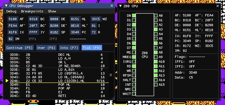
The Z80-based Tiny Emulators have all been updated to the new cycle-stepped model, which also means that the CPU step debugger now supports cycle-stepping (which is very useful for debugging the other chips in the emulated system):
…also, if you haven’t seen it yet, check out the Visual Z80 Remix project, which I did as preparation for the new Z80 emulator to get the cycle timing right and better understand what’s going on in some of the more esoteric instructions.
A Code Sample
Here’s a simple code example to get an idea how the new emulator works:
#include <stdio.h>
#define CHIPS_IMPL
#include "z80.h"

int main() {
    // 64 KB memory with test program at address 0x0000
    uint8_t mem[(1<<16)] = {
        0x3E, 0x02,     // LD A,2
        0x06, 0x03,     // LD B,3
        0x80,           // ADD A,B
        0x00,           // NOP...
    };

    // initialize Z80 emu and execute some clock cycles
    z80_t cpu;
    uint64_t pins = z80_init(&cpu);
    for (int i = 0; i < 20; i++) {

        // tick the CPU
        pins = z80_tick(&cpu, pins);

        // handle memory read or write access
        if (pins & Z80_MREQ) {
            if (pins & Z80_RD) {
                Z80_SET_DATA(pins, mem[Z80_GET_ADDR(pins)]);
            }
            else if (pins & Z80_WR) {
                mem[Z80_GET_ADDR(pins)] = Z80_GET_DATA(pins);
            }
        }
    }

    // register A should now be 5
    printf("\nRegister A: %d\n", cpu.a);
    return 0;
}
Here’s the same code on Compiler Explorer.
The emulator only has two important API functions:
uint64_t z80_init(z80_t* cpu)
…this initializes a Z80 instance and returns an ‘ignition pin bitmask’ which is passed into the first tick function call:
uint64_t z80_tick(z80_t* cpu, uint64_t pins)
…the tick function executes exactly one clock cycle and then returns to the caller with a modified pin bitmask. This bitmask is used to communicate with the ‘outside world’ just like the input/output pins on a real CPU.
The caller inspects the returned pin mask (for instance to check if the CPU wants to read
or write memory), modifies the pin mask accordingly, and feeds it back into the next
call of z80_tick(). And that’s it, no more ‘system tick callback’, or
‘trace callback’ for debugger support like in the old Z80 emulator.
Basic Implementation Ideas
Instruction decoding happens in a big switch-case statement like in the previous emulator, but instead of one case-branch per opcode there’s now one case branch per instruction clock cycle.
In the new emulator, the decoder switch-case statement looks more like a program which implements its own ‘meta control flow’.
A simple sequence where each call to the tick function executes the next step would look like this:
void tick(state_t* state) {
    switch (state->step++) {
        case 0: ... break;
        case 1: ... break;
        case 2: ... break;
        ...
    }
}
Calling such a tick function over and over would first step through all the case branches until there are no more branches left or the step counter overflows.
To implement an unconditional branch the step counter is simply set to the destination step, so that execution continues there on the next call of the tick function.
For instance here the step counter is reset to zero at the end of the sequence, implementing an infinite loop:
void tick(state_t* state) {
    switch (state->step++) {
        case 0: ... break;
        case 1: ... break;
        case 2: ... break;
        case 3: state->step = 0; break;
    }
}
Calling the tick function will now execute the steps 0..3 forever: [0, 1, 2, 3, 0, 1, 2, 3, …].
Of course branches can also jump forward to skip steps:
void tick(state_t* state) {
    switch (state->step++) {
        case 0: ... break;
        case 1: state->step = 3; break;
        case 2: ... break;
        case 3: state->step = 0; break;
    }
}
Step 2 will now always be skipped, resulting in [0, 1, 3, 0, 1, 3, …].
…and conditional branches only modify the step counter when a condition is true:
void tick(state_t* state) {
    switch (state->step++) {
        case 0: state->cond = !state->cond; break;
        case 1: if (state->cond) { state->step = 3; } break;
        case 2:     ... break;
        case 3: state->step = 0; break;
    }
}
Because state->cond is now toggled in step 0, step 2 will be skipped in every other ‘run’ of the program: [0, 1, 3, 0, 1, 2, 3, 0, 1, 3, …].
Code that needs to be executed on each call of the tick function can be placed in front (prologue) or after (epilogue) the switch-case statement:
void tick(state_t* state) {
    prologue;
    switch (state->step++) {
        case 0: state->cond = !state->cond; break;
        case 1: if (state->cond) { state->step = 3; } break;
        case 2:     ... break;
        case 3: state->step = 0; break;
    }
    epilogue;
}
And finally, in C we can “break into” different epilogue code blocks using the good old goto statement:
void tick(state_t* state) {
    prologue;
    switch (state->step++) {
        case 0: state->cond = !state->cond; goto ep_1;
        case 1: if (state->cond) { state->step = 3; } goto ep_1;
        case 2:     ...; goto ep_2;
        case 3: state->step = 0; goto ep_1;
    }
ep_1:
    epilogue_1;
ep_2:
    epilogue_2;
}
Now the steps 0, 1 and 3 will run epilogue_1 and epilogue_2 on function
exit, but step 2 will only execute epilogue_2.
With the above core ideas it’s now possible to encode Z80 instructions into switch-case ‘microcode’:
For example, the LD HL,nn instruction loads a 16-bit immediate value into the register pair HL. Execution of the instruction takes 10 clock cycles, split into 3 machine cycle groups:
- opcode fetch and refresh (4 clock cycles)
- read low byte into L (3 clock cycles)
- read high byte into H (3 clock cycles)
…encoded into a switch-case sequence (as simplified pseudocode, abus and dbus means ‘address bus’ and ‘data bus’):
uint64_t tick(z80_t* cpu, uint64_t pins) {
    switch (cpu->step++) {
        // opcode fetch + refresh machine cycle
        case 0: pins = (M1|MREQ|RD) | set_abus(cpu->PC++); break;
        case 1: cpu->opcode = get_dbus(pins); break;
        case 2: pins = (RFSH|MREQ) | set_abus(...); break;
        case 3: break;

        // first read machine cycle
        case 4: break;
        case 5: pins = (MREQ|RD) | set_abus(cpu->pc++); break;
        case 6: cpu->L = get_dbus(pins); break;

        // second read machine cycle
        case 7: break;
        case 8: pins = (MREQ|RD) | set_abus(cpu->pc++); break;
        case 9: cpu->H = get_dbus(pins); cpu->step = 0; break;
    }
}
This looks pretty good already, but there’s a chicken-egg-problem: the opcode fetch machine cycle (the first four steps) doesn’t actually do anything. Even though it loads an opcode byte, the opcode is ignored and the CPU will only ever execute LD HL,nn instructions. Currently there’s no way to add additional instructions to the switch statement.
The solution is to split the switch-case decoder into a shared opcode fetch machine cycle which is the same for all instructions, and then do a branch to the remaining steps (which I’ll call ‘the instruction payload’ henceforth) somewhere else in the big switch-case statement.
At the end of the shared opcode fetch machine cycle, a table lookup
is performed with the opcode as index which yields the first step
of the instruction payload (look at case 3:):
uint64_t tick(z80_t* cpu, uint64_t pins) {
    switch (cpu->step++) {
        // opcode fetch + refresh machine cycle
        case 0: pins = (M1|MREQ|RD) | set_abus(cpu->PC++); break;
        case 1: cpu->opcode = get_dbus(pins); break;
        case 2: pins = (RFSH|MREQ) | set_abus(...); break;
        case 3: cpu->step = cpu->opstep[cpu->opcode];

        ...

        // somewhere else in the big switch-case:
        // first read machine cycle of LD HL,nn
        case N+0: break;
        case N+1: pins = (MREQ|RD) | set_abus(cpu->pc++); break;
        case N+2: cpu->L = get_dbus(pins); break;

        // second read machine cycle of LD HL,nn
        case N+3: break;
        case N+4: pins = (MREQ|RD) | set_abus(cpu->pc++); break;
        case N+5: cpu->H = get_dbus(pins); cpu->step = 0; break;

        ...
    }
}
Note how the last step at case (N+5) loops back to step 0 to load the next opcode byte. In general, that’s how the cycle-stepped emulation loop works, but there’s one last problem: most instructions in the Z80 instruction set take 4 cycles to execute, but this doesn’t fit into the above execution pattern.
Since the opcode fetch machine cycle already takes 4 clock cycles, there’s no clock cycle left to execute the instruction payload.
Let’s take the ADD A,B instruction as example, this should look like this:
uint64_t tick(z80_t* cpu, uint64_t pins) {
    switch (cpu->step++) {
        // opcode fetch + refresh machine cycle
        case 0: pins = (M1|MREQ|RD) | set_abus(cpu->PC++); break;
        case 1: cpu->opcode = get_dbus(pins); break;
        case 2: pins = (RFSH|MREQ) | set_abus(...); break;
        case 3: cpu->step = cpu->opstep[cpu->opcode];

        ...

        // ADD A,B payload:
        case N: cpu->a=add8(cpu->a,cpu->b); cpu->step=0; break;

        ...
    }
}
But this would take 5 clock cycles, not the required 4.
The solution is to use the same trick as a real-world Z80: overlap the
execution of the last instruction with the opcode fetch of the next instruction
by merging the last instruction clock cycle with the first clock cycle of
the next opcode fetch, note how the old case 0: step has been removed and
merged with the ADD A,B payload step:
uint64_t tick(z80_t* cpu, uint64_t pins) {
    switch (cpu->step++) {
        // last 3 clock cyles of opcode fetch + refresh machine cycle
        case 0: cpu->opcode = get_dbus(pins); break;
        case 1: pins = (RFSH|MREQ) | set_abus(...); break;
        case 2: cpu->step = cpu->opstep[cpu->opcode];

        ...
        // ADD A,B payload:
        case N:
            cpu->a=add8(cpu->a,cpu->b);
            pins = (M1|MREQ|RD) | set_abus(cpu->PC++);
            cpu->step = 0;
            break;
        ...
    }
}
…it looks a bit nicer when wrapping the actions of the first opcode fetch cycle into a macro:
#define _fetch() {pins=(M1|MREQ|RD)|set_abus(cpu->PC++);cpu->step=0}

uint64_t tick(z80_t* cpu, uint64_t pins) {
    switch (cpu->step++) {
        // last 3 clock cyles of opcode fetch + refresh machine cycle
        case 0: cpu->opcode = get_dbus(pins); break;
        case 1: pins = (RFSH|MREQ) | set_abus(...); break;
        case 2: cpu->step = cpu->opstep[cpu->opcode];

        ...
        // ADD A,B payload and first clock cycle of next opcode fetch
        case N+0: cpu->a=add8(cpu->a,cpu->b); _fetch(); break;
        ...
    }
}
With this overlap-trick the timing for 4-cycle instruction is working fine now.
You might be wondering now how the very first instruction starts executing. The
trick is that the z80_init() function doesn’t initialize the
cpu->step to 0, but instead to the overlapped payload-and-fetch clock
cycle of the NOP instruction. That way the CPU emulation is properly ‘ignited’
at the first call to the z80_tick() function.
The only problem left to figure out now is how to ‘draw the rest of the f*cking owl’.
Code Generation
Like in my previous CPU emulators, I’m using a Python script to generate the instruction decoder C source code. But this time I tried another idea that was also rolling around in the back of my head for a long time: instead of hardwiring the instruction behaviour and timing entirely in the Python script, describe the instructions in a data file, and process that data file with a much smaller and more general Python script.
I’m using YAML as file format for this data file. YAML isn’t perfect because it requires the separately installed PyYAML dependency, but apart from that it’s quite alright for this use case.
The YAML file contains instruction descriptions like this:
LD $RY,$RZ:
  cond: (x == 1) and (y != 6) and (z != 6)
  mcycles:
    - { type: overlapped,  action: $RY=$RZ }
Those 4 lines describe all 49 instructions for loading an 8-bit register into
another. The cond: line is a python expression matching the 2-3-3 opcode
bit pattern described here:
Identifiers starting with $ are placeholders which will be replaced with concrete register names or C code snippets during code generation.
Machine cycles with default timing are implicit and don’t need to be listed (for instance in this case the opcode fetch machine cycle).
The generated code will look like this (for the LD A,B instruction):
        //  78: LD A,B (M:1 T:4)
        // -- overlapped
        case  399: cpu->a=cpu->b;goto fetch_next;
Another more interesting example is the LD dd,nn instruction group, which loads the 16-bit immediate value nn into register pair dd.
The YAML description looks like this:
# 16-bit load immediate/add
LD $RP,nn:
  cond: (x == 0) and (z == 1) and (q == 0)
  mcycles:
    - { type: mread,  ab: $PC++, dst: $RPL }
    - { type: mread,  ab: $PC++, dst: $RPH }
Again, the opcode fetch machine cycle has default behaviour and isn’t listed, and this instruction also doesn’t overlap execution with the next instruction. What remains are two memory read machine cycles to load the 16-bit value from memory into the destination register pair.
The stamped out C code for LD DE,nn looks like this:
        //  11: LD DE,nn (M:3 T:10)
        // -- mread
        case   83: goto step_next;
        case   84: _wait();_mread(cpu->pc++);goto step_next;
        case   85: cpu->e=_gd();goto step_next;
        // -- mread
        case   86: goto step_next;
        case   87: _wait();_mread(cpu->pc++);goto step_next;
        case   88: cpu->d=_gd();goto step_next;
        // -- overlapped
        case   89: goto fetch_next;
The macro _mread() sets the CPU pins for a memory read machine cycle (MREQ|RD and address
bus pins).
The macro _gd() extracts the data bus pins into an uint8_t. The _wait() macro
samples the WAIT pin and will be explained later.
The code generation Python script is now just around 400 lines of code, compared to about 1000 lines for the old script. However, when counting lines for all involved files (a C header template file, the Python script, and the YAML file) the old and new approach is nearly identical (1691 C+YAML+Python for the new approach, and 1633 lines C+Python for the old approach).
One clear advantage of the new approach is that the same YAML description file can be used for different code generation scripts (for instance the instruction tables in my last blog post have been generated from the same data with a different generator script).
It will also be much easier to quickly try out different decoder ideas in the future.
You can take a look at all involved source files for code generation here:
…and the resulting code-generated header:
The Shared Opcode Fetch Machine Cycle
The shared code for an opcode fetch machine cycle looks like this:
        // M1/T2: load opcode from data bus
        case 0: _wait(); cpu->opcode = _gd(); goto step_next;
        // M1/T3: refresh cycle
        case 1: pins = _z80_refresh(cpu, pins); goto step_next;
        // M1/T4: branch to instruction payload
        case 2: {
            cpu->step = _z80_optable[cpu->opcode];
            // preload effective address for (HL) ops
            cpu->addr = cpu->hl;
        } goto step_next;
These are only the last 3 of 4 clock cycles: As explained earlier, the ‘missing’ first clock cycle is overlapped with the last instruction clock cycle and is part of the specific instruction payload decoder blocks elsewhere in the big switch-case statement.
In the first step, the WAIT pin is sampled (and if set, execution will be stuck on this decoder step - more details on wait state behaviour later in the post). If the WAIT pin isn’t active, the opcode byte is loaded from the data bus.
The _z80_refresh() function sets the pins for a refresh cycle (MREQ|RFSH)
and the address bus pins to a 16-bit value formed from the I and R register
pair. The lower 7 bits in the R register are incremented, while the topmost bit
remains unchanged. The refresh cycle normally has no use in system emulators
apart from the side effect of the R register counting up (unless of course one
would like to implement “DRAM decay”).
The last clock cycle in the opcode fetch machine cycle branches to the instruction payload by doing a table lookup with the previously loaded opcode byte as index. Finally, the ‘effective address’ is preloaded with the content of the HL register (which is only needed for instructions involving (HL)).
The Opcode Lookup Tables
Apart from the big switch-case decoder, three lookup tables of 256 entries each are code-generated which are indexed with the opcode byte. The lookup yields the decoder switch-case step of the instruction payload.
The three opcode tables are:
- The main instruction block for unprefixed instructions.
- A variation of the main instruction block for DD/FD prefixed instructions, this table is identical with the main table, except for instructions that involve (HL): those are modified into (IX+d) or (IY+d) and need to branch to an ‘interlude decoder block’ which loads the d-offset and computes the effective address before continuing with the actual instruction payload.
- And finally a separate opcode lookup table for the ED prefixed instructions.
One would expect a fourth table for the CB-prefixed instruction block, but since this instruction block can easily be decoded algorithmically I decided to handle this as a special case.
Opcode tables are just simple uint16_t arrays:
static const uint16_t _z80_optable[256] = {
      27,  // 00: NOP (M:1 T:4 steps:1)
      28,  // 01: LD BC,nn (M:3 T:10 steps:7)
      35,  // 02: LD (BC),A (M:2 T:7 steps:4)
      39,  // 03: INC BC (M:2 T:6 steps:3)
      42,  // 04: INC B (M:1 T:4 steps:1)
      43,  // 05: DEC B (M:1 T:4 steps:1)
      44,  // 06: LD B,n (M:2 T:7 steps:4)
      48,  // 07: RLCA (M:1 T:4 steps:1)
      ...
     930,  // FC: CALL M,nn (M:6 T:17 steps:14)
     944,  // FD: FD prefix (M:1 T:4 steps:1)
     945,  // FE: CP n (M:2 T:7 steps:4)
     949,  // FF: RST 38h (M:4 T:11 steps:8)
 };
The stored step index is the actual decoder step - 1, because the decoder step is ‘post-incremented’ in the tick function epilogue. For instance the LD BC,nn instruction which has the opcode byte 0x01 has the decoder step 28 stored in the opcode table, which - post-incremented by one - points to the instruction payload block at decoder step 29:
        //  01: LD BC,nn (M:3 T:10)
        // -- mread
        case   29: goto step_next;
        case   30: _wait();_mread(cpu->pc++);goto step_next;
        case   31: cpu->c=_gd();goto step_next;
        // -- mread
        case   32: goto step_next;
        case   33: _wait();_mread(cpu->pc++);goto step_next;
        case   34: cpu->b=_gd();goto step_next;
        // -- overlapped
        case   35: goto fetch_next;
The 3 Tick Function Epilogues
…about all those gotos: the epilogue at the end of the z80_tick() function looks like this:
fetch_next: pins = _z80_fetch(cpu, pins);
step_next:  cpu->step += 1;
track_int_bits: {
        // track NMI 0 => 1 edge and current INT pin state, this will track the
        // relevant interrupt status up to the last instruction cycle and will
        // be checked in the first M1 cycle (during _fetch)
        const uint64_t rising_nmi = (pins ^ cpu->pins) & pins; // NMI 0 => 1
        cpu->pins = pins;
        cpu->int_bits = ((cpu->int_bits | rising_nmi) & Z80_NMI) | (pins & Z80_INT);
    }
    return pins;
There are 3 ‘cascaded’ labels which fall through to the next label. Let’s start at the last label:
The main job of the code block under track_int_bits: is to track the NMI and INT pins for interrupt detection. More on this later in a dedicated section about interrupt handling. The interrupt pin tracking needs to happen in every clock cycle, that’s why it is in the last fallthrough position.
Next up is the step_next: label. This simply increments the step counter by 1 and needs to happen in each clock cycle, unless the CPU is executing WAIT cycles.
And finally the fetch_next: label initiates an opcode fetch for the next instruction.
The reason why those shared epilogue code blocks and gotos exist is ‘manual code deduplication’. It would just as well be possible to add those code blocks to each case branch, but that’s a lot of duplicated code. A smart compiler might be able to do the same deduplication, but depending on this was a bit beyond my personal “acceptable compiler magic” threshold.
More on Wait Cycles
Machine cycles which access memory or IO ports need to sample the WAIT pin in specific clock cycles. If the WAIT pin is active, the CPU stops regular execution until the WAIT pin goes inactive again. This allows the CPU to wait for slow memory or peripheral devices, but in some computer systems (like the Amstrad CPC) wait cycles are used to synchronize memory access between the CPU and video hardware, which is why it is important to get the wait timing right.
In the emulation, a _wait() macro is inserted at the start of case branches where the WAIT pin needs to be sampled. In regular memory read and write machine cycles this is the second clock cycle, and in IO read or write machine cycles the third clock cycle. Wait sampling also needs to happen during opcode fetch, and in interrupt acknowledge cycles.
Here’s for example a typical memory read machine cycle:
        case 17: goto step_next;
        case 18: _wait();_mread(cpu->pc++); goto step_next;
        case 19: cpu->dlatch=_gd(); goto step_next;
The _wait() macro simply expands to:
if (pins & Z80_WAIT) {
    goto track_int_bits;
}
Jumping to the track_int_bits: epilogue label skips the decoder step increment, so
the next time the z80_tick() function is called, execution continues at
the same case-branch which first checks the WAIT pin state. Only when the WAIT
pin is no longer active, regular execution continues.
Instructions with Variable Timing
Some conditional branch instructions take less cycles to execute if the branch is not taken, for instance the conditional relative branch instruction JR cc,d.
If the condition is true (branch taken) the instruction takes 12 clock cycles, but if the branch is not taken only 7 clock cycles.
In the emulation this is implemented by skipping to the overlapped clock cycle at the end of the instruction payload (look at case 176):
        //  28: JR Z,d (M:3 T:12)
        // -- mread
        case  174: goto step_next;
        case  175: _wait();_mread(cpu->pc++);goto step_next;
        case  176: cpu->dlatch=_gd();if(!(_cc_z)){_skip(5);};goto step_next;
        // -- generic
        case  177: cpu->pc+=(int8_t)cpu->dlatch;cpu->wz=cpu->pc;goto step_next;
        case  178: goto step_next;
        case  179: goto step_next;
        case  180: goto step_next;
        case  181: goto step_next;
        // -- overlapped
        case  182: goto fetch_next;
The _skip(5) macro in step 176 simply expands to:
cpu->step+=5;
The ‘Overlapped Clock Cycle’ in more Detail
The last clock cycle in an instruction decoder block (which is actually the first clock cycle of the next opcode fetch machine cycle) mainly sets the CPU pins to load the next opcode byte:
- The
M1|MREQ|RDpins are set. - The address bus is loaded with the program counter and the program counter is incremented.
- The decoder step is set to 0xFFFF, which will overflow to 0 when the step counter is incremented at the end of the tick function so that in the next tick function call execution continues at the first step of the shared opcode fetch decoder block.
The other important thing that needs to happen in the overlapped clock cycle is interrupt detection. On a real Z80, interrupt detection happens in the last clock cycle of an instruction, but in the emulator it made more sense to move the interrupt detection code out of the instruction-specific payload block and into the shared opcode fetch preparation code.
Interrupt handling will be explained in more details later in the blog post.
DD/FD Prefix Handling
The DD and FD opcodes execute as regular 4-cycle instructions, but with a slightly
modified overlapped clock cycle: Instead of jumping to the common fetch_next: label
a special opcode fetch is initiated:
        //  DD: DD prefix (M:1 T:4)
        // -- overlapped
        case  726: _fetch_dd();goto step_next;
        ...
        //  FD: FD prefix (M:1 T:4)
        // -- overlapped
        case  945: _fetch_fd();goto step_next;
The macros _fetch_dd() and _fetch_fd() expand to functions calls:
#define _fetch_dd()     pins=_z80_fetch_dd(cpu,pins);
#define _fetch_fd()     pins=_z80_fetch_fd(cpu,pins);
…which in turn look like this:
static inline uint64_t _z80_fetch_dd(z80_t* cpu, uint64_t pins) {
    cpu->step = 2;   // => step 3: opcode fetch for DD/FD prefixed instructions
    cpu->hlx_idx = 1;
    cpu->prefix_active = true;
    return _z80_set_ab_x(pins, cpu->pc++, Z80_M1|Z80_MREQ|Z80_RD);
}

static inline uint64_t _z80_fetch_fd(z80_t* cpu, uint64_t pins) {
    cpu->step = 2;   // => step 3: opcode fetch for DD/FD prefixed instructions
    cpu->hlx_idx = 2;
    cpu->prefix_active = true;
    return _z80_set_ab_x(pins, cpu->pc++, Z80_M1|Z80_MREQ|Z80_RD);
}
The first important difference to the regular _z80_fetch() function is that no interrupt detection happens (because interrupts are not handled after fetching prefix bytes).
prefix_active can be ignored, this is only used by
the helper function z80_opdone() to test whether an instruction has finished
executing (which is only needed for test code or implementing debuggers).
The returned pinmask is identical with a regular opcode fetch: The pins M1|MREQ|RD
are set to active, and the program counter is put on the address bus and incremented.
The hlx_idx index is used for the HL => IX/IY register-renaming taking place in DD/FD prefixed instructions through the following somewhat scary nested union in struct z80_t:
    union {
        struct {
            union { struct { uint8_t l; uint8_t h; }; uint16_t hl; };
            union { struct { uint8_t ixl; uint8_t ixh; }; uint16_t ix; };
            union { struct { uint8_t iyl; uint8_t iyh; }; uint16_t iy; };
        };
        struct { union { struct { uint8_t l; uint8_t h; }; uint16_t hl; }; } hlx[3];
    };
The upper part allows to directly access the 8-bit registers L, H, IXL, IXH, IYL and IYH, or the 16-bit register pairs HL, IX and IY.
The hlx[3] array allows to access the same registers through an index:
    cpu->hlx[0].l => L
    cpu->hlx[0].h => H
    cpu->hlx[0].hl => HL

    cpu->hlx[1].l => IXL
    cpu->hlx[1].h => IXH
    cpu->hlx[1].hl => IX

    cpu->hlx[2].l => IYL
    cpu->hlx[2].h => IYH
    cpu->hlx[2].hl => IY
For regular, unprefixed instructions the register renaming index (hlx_idx) is set to 0, so that register pair HL is accessed.
For DD-prefixed instruction the index is set to 1, which accesses IX, and for FD-prefixed instructions the index is set to 2, which accesses IY.
Instructions which ignore the HL/IX/IY register renaming (such as EX HL,DE) simply access the item cpu->hl directly without going through the cpu->hlx[cpu->hlx_idx] indirection.
The last and most important difference to a regular opcode fetch is that the decoder step is set to 2 instead of 0xFFFF. This means that on the next call to the tick function, execution continues not at the regular shared opcode fetch decoder block, but at a special decoder block at step 3:
        //=== shared fetch machine cycle for DD/FD-prefixed ops
        // M1/T2: load opcode from data bus
        case 3: _wait(); cpu->opcode = _gd(); goto step_next;
        // M1/T3: refresh cycle
        case 4: pins = _z80_refresh(cpu, pins); goto step_next;
        // M1/T4: branch to instruction payload
        case 5: {
            cpu->step = _z80_ddfd_optable[cpu->opcode];
            cpu->addr = cpu->hlx[cpu->hlx_idx].hl;
        } goto step_next;
The first difference to a regular opcode fetch is how the ‘effective address’ is preloaded in step 5:
Instead of loading addr with HL, the register renaming index hlx_idx is used, which causes either the IX or IY register to be loaded into addr, depending on the previously ‘executed’ prefix-byte instruction (DD or FD):
cpu->addr = cpu->hlx[cpu->hlx_idx].hl;
The next difference is that the instruction payload step is looked up from a different table: _z80_ddfd_optable[] instead of _z80_optable[]. The _z80_ddfd_optable[] is identical to the regular optable, except for instructions that involve (HL) which need to be modified to (IX+d) or (IY+d).
Those instructions will ‘inject’ a decoder block after the opcode fetch machine cycle which loads the d offset, adds it to the ‘effective address’, and then continues to the original instruction decoder block:
        //=== optional d-loading cycle for (IX+d), (IY+d)
        //--- mread
        case 6: goto step_next;
        case 7: _wait();_mread(cpu->pc++); goto step_next;
        case 8: cpu->addr += (int8_t)_gd(); cpu->wz = cpu->addr; goto step_next;
        //--- filler ticks
        case 9: goto step_next;
        case 10: goto step_next;
        case 11: goto step_next;
        case 12: goto step_next;
        case 13: {
            // branch to actual instruction
            cpu->step = _z80_optable[cpu->opcode];
        } goto step_next;
All taken together this means that the instruction LD A,(IX+3) executes the following decoder step sequence (starting with the opcode fetch for the DD prefix), note how the execution jumps between entirely different parts of the decoder switch-case statement:
        //=== shared fetch machine cycle for non-DD/FD-prefixed ops
        // M1/T2: load opcode from data bus
        case 0: _wait(); cpu->opcode = _gd(); goto step_next;
        // M1/T3: refresh cycle
        case 1: pins = _z80_refresh(cpu, pins); goto step_next;
        // M1/T4: branch to instruction payload
        case 2: {
            cpu->step = _z80_optable[cpu->opcode];
            // preload effective address for (HL) ops
            cpu->addr = cpu->hl;
        } goto step_next;

        //  DD: DD prefix (M:1 T:4)
        // -- overlapped
        case  726: _fetch_dd();goto step_next;

        //=== shared fetch machine cycle for DD/FD-prefixed ops
        // M1/T2: load opcode from data bus
        case 3: _wait(); cpu->opcode = _gd(); goto step_next;
        // M1/T3: refresh cycle
        case 4: pins = _z80_refresh(cpu, pins); goto step_next;
        // M1/T4: branch to instruction payload
        case 5: {
            cpu->step = _z80_ddfd_optable[cpu->opcode];
            cpu->addr = cpu->hlx[cpu->hlx_idx].hl;
        } goto step_next;

        //=== optional d-loading cycle for (IX+d), (IY+d)
        //--- mread
        case 6: goto step_next;
        case 7: _wait();_mread(cpu->pc++); goto step_next;
        case 8: cpu->addr += (int8_t)_gd(); cpu->wz = cpu->addr; goto step_next;
        //--- filler ticks
        case 9: goto step_next;
        case 10: goto step_next;
        case 11: goto step_next;
        case 12: goto step_next;
        case 13: {
            // branch to actual instruction
            cpu->step = _z80_optable[cpu->opcode];
        } goto step_next;

        //  7E: LD A,(HL) (M:2 T:7)
        // -- mread
        case  405: goto step_next;
        case  406: _wait();_mread(cpu->addr);goto step_next;
        case  407: cpu->a=_gd();goto step_next;
        // -- overlapped
        case  408: goto fetch_next;
This adds up to 19 decoder steps or clock cycles, and that’s indeed the duration of the LD A,(IX+d) instruction.
There is one special case in the _z80_ddfd_optable[] and that is the LD (HL),n instruction which is modified to LD (IX+d),n or LD (IY+d),n. This is the only instruction which doesn’t simply insert 8 clock cycles for loading the d-offset and computing the effective address, instead it overlays the memory read machine cycle for loading the immediate value n over those 8 extra clock cycles.
This is handled with a special d-loading decoder block, which then jumps into the middle of the original LD (HL),n payload.
The special d/n-loading decoder block looks like this:
        //=== special case d-loading cycle for (IX+d),n where the immediate load
        //    is hidden in the d-load cycle
        //--- mread for d offset
        case 14: goto step_next;
        case 15: _wait();_mread(cpu->pc++); goto step_next;
        case 16: cpu->addr += (int8_t)_gd(); cpu->wz = cpu->addr; goto step_next;
        //--- mread for n
        case 17: goto step_next;
        case 18: _wait();_mread(cpu->pc++); goto step_next;
        case 19: cpu->dlatch=_gd(); goto step_next;
        //--- filler tick
        case 20: goto step_next;
        case 21: {
            // branch to ld (hl),n and skip the original mread cycle for loading 'n'
            cpu->step = _z80_optable[cpu->opcode] + 3;
        } goto step_next;
…execution then continues at the memory write machine cycle of LD (HL),n which writes the immediate value n back to the memory location defined by the ‘effective address’:
        //  36: LD (HL),n (M:3 T:10)
        ...
        // -- mwrite
        case  262: goto step_next;
        case  263: _wait();_mwrite(cpu->addr,cpu->dlatch);goto step_next;
        case  264: goto step_next;
        // -- overlapped
        case  265: goto fetch_next;
ED Prefix Handling
Just as the other prefix instructions, the ED instruction executes as regular 4-clock-cycle instruction but calls into a special opcode fetch function in the overlapped clock cycle:
        //  ED: ED prefix (M:1 T:4)
        // -- overlapped
        case  842: _fetch_ed();goto step_next;
The _fetch_ed() macro expands to:
static inline uint64_t _z80_fetch_ed(z80_t* cpu, uint64_t pins) {
    cpu->step = 24; // => step 25: opcode fetch for ED prefixed instructions
    cpu->hlx_idx = 0;
    cpu->prefix_active = true;
    return _z80_set_ab_x(pins, cpu->pc++, Z80_M1|Z80_MREQ|Z80_RD);
}
This looks very much like the _z80_fetch_ddfd() function above. No interrupts are handled, the decoder step is set to a special opcode fetch machine cycle and the returned pin mask initiates a standard opcode fetch.
The hlx_idx register renaming index is reset to zero. This means that the ED prefix cancels the effect of the DD and FD prefixes (e.g. HL is never renamed to IX or IY in ED-prefixed instructions).
The special ED opcode fetch machine cycle uses a different opcode lookup table _z80_ed_optable[], this points to all the ED-prefixed instruction payload steps:
        //=== special opcode fetch machine cycle for ED-prefixed instructions
        // M1/T2: load opcode from data bus
        case 25: _wait(); cpu->opcode = _gd(); goto step_next;
        // M1/T3: refresh cycle
        case 26: pins = _z80_refresh(cpu, pins); goto step_next;
        // M1/T4: branch to instruction payload
        case 27: cpu->step = _z80_ed_optable[cpu->opcode]; goto step_next;
CB Prefix Handling
CB prefix handling starts like the other prefixes: with a separate fetch macro in the overlapped step:
        //  CB: CB prefix (M:1 T:4)
        // -- overlapped
        case  583: _fetch_cb();goto step_next;
The macro _fetch_cb() wraps this function:
static inline uint64_t _z80_fetch_cb(z80_t* cpu, uint64_t pins) {
    cpu->prefix_active = true;
    if (cpu->hlx_idx > 0) {
        // this is a DD+CB / FD+CB instruction, continue
        // execution on the special DDCB/FDCB decoder block which
        // loads the d-offset first and then the opcode in a
        // regular memory read machine cycle
        cpu->step = _z80_special_optable[_Z80_OPSTATE_SLOT_DDFDCB];
    }
    else {
        // this is a regular CB-prefixed instruction, continue
        // execution on a special fetch machine cycle which doesn't
        // handle DD/FD prefix and then branches either to the
        // special CB or CBHL decoder block
        cpu->step = 21; // => step 22: opcode fetch for CB prefixed instructions
        pins = _z80_set_ab_x(pins, cpu->pc++, Z80_M1|Z80_MREQ|Z80_RD);
    }
    return pins;
}
…this however looks quite a bit different than the DD/FD or ED prefixes!
Long story short: since the CB-prefixed instruction block is very ‘orderly’ (see my previous blog post for details) I decided to decode the entire CB instruction block in a single function and a handful of special instruction decoder blocks.
For instance all CB-prefixed instructions that don’t involve (HL) execute the following sequence of decoder steps:
        //=== special opcode fetch machine cycle for CB-prefixed instructions
        case 22: _wait(); cpu->opcode = _gd(); goto step_next;
        case 23: pins = _z80_refresh(cpu, pins); goto step_next;
        case 24: {
            if ((cpu->opcode & 7) == 6) {
                // not taken:
                // this is a (HL) instruction
                ...
            }
            else {
                cpu->step = _z80_special_optable[_Z80_OPSTATE_SLOT_CB];
            }
        } goto step_next;

        ...

        // CB 00: cb (M:1 T:4)
        // -- overlapped
        case 1437: {uint8_t z=cpu->opcode&7;_z80_cb_action(cpu,z,z);};goto fetch_next;
_z80_cb_action() is the magic function which decodes and implements all Z80 instructions in the CB-prefix instruction block (here’s the implementation).
CB-prefixed instructions which involve (HL) have a more complex payload for reading and (optionally) writing back the operand:
        //=== special opcode fetch machine cycle for CB-prefixed instructions
        case 22: _wait(); cpu->opcode = _gd(); goto step_next;
        case 23: pins = _z80_refresh(cpu, pins); goto step_next;
        case 24: {
            if ((cpu->opcode & 7) == 6) {
                // this is a (HL) instruction
                cpu->addr = cpu->hl;
                cpu->step = _z80_special_optable[_Z80_OPSTATE_SLOT_CBHL];
            }
            else {
                // not taken
                ...
            }
        } goto step_next;

        ...

        // CB 00: cbhl (M:3 T:11)
        // -- mread
        case 1438: goto step_next;
        case 1439: _wait();_mread(cpu->hl);goto step_next;
        case 1440: cpu->dlatch=_gd();if(!_z80_cb_action(cpu,6,6)){_skip(3);};goto step_next;
        case 1441: goto step_next;
        // -- mwrite
        case 1442: goto step_next;
        case 1443: _wait();_mwrite(cpu->hl,cpu->dlatch);goto step_next;
        case 1444: goto step_next;
        // -- overlapped
        case 1445: goto fetch_next;
The memory write machine cycle which writes back the result is skipped if the _z80_cb_action() function returns true (which happens if this is a bit-testing instruction).
Finally, the weird DD/FD + CB double-prefixed instructions are handled through another special decoder block which looks like this:
        // CB 00: ddfdcb (M:6 T:18)
        case 1446: _wait();_mread(cpu->pc++);goto step_next;
        case 1447: _z80_ddfdcb_addr(cpu,pins);goto step_next;
        // -- mread
        case 1448: goto step_next;
        case 1449: _wait();_mread(cpu->pc++);goto step_next;
        case 1450: cpu->opcode=_gd();goto step_next;
        case 1451: goto step_next;
        case 1452: goto step_next;
        // -- mread
        case 1453: goto step_next;
        case 1454: _wait();_mread(cpu->addr);goto step_next;
        case 1455: cpu->dlatch=_gd();if(!_z80_cb_action(cpu,6,cpu->opcode&7)){_skip(3);};goto step_next;
        case 1456: goto step_next;
        // -- mwrite
        case 1457: goto step_next;
        case 1458: _wait();_mwrite(cpu->addr,cpu->dlatch);goto step_next;
        case 1459: goto step_next;
        // -- overlapped
        case 1460: goto fetch_next;
This needs some explanation:
Instead of a regular opcode fetch machine cycle, execution starts with a memory read machine cycle (just the last two cycles because the previous step was the usual overlapped clock cycle of the CB prefix).
This memory read machine cycle loads the d-offset and then computes the effective address (IX+d) or (IY+d) in the helper function _z80_ddfdcb_addr():
// compute the effective memory address for DD+CB/FD+CB instructions
static inline void _z80_ddfdcb_addr(z80_t* cpu, uint64_t pins) {
    uint8_t d = _z80_get_db(pins);
    cpu->addr = cpu->hlx[cpu->hlx_idx].hl + (int8_t)d;
    cpu->wz = cpu->addr;
}
Next in step 1448, a regular memory read machine cycle loads the actual opcode
byte into cpu->opcode (so the opcode byte isn’t loaded with an opcode
fetch machine cycle, but instead with a memory read machine cycle - this is
also why the R register is only incremented twice during a DD/FD+CB
instruction: there are only two ‘proper’ opcode fetch machine cycles for the
DD/FD prefix and the CB prefix).
The next memory read machine cycle loads the operand byte from the effective address (IX+d or IY+d), and performs the actual payload action of the instruction in the _z80_cb_action() function, which will also write the result into a register if needed (this is the case for the undocumented instructions which write the result both into a register and to memory). If the instruction was a bit-testing instruction, the following memory write machine cycle is skipped.
Interrupt Detection
On a real Z80, interrupts are detected in the last clock cycle of an instruction (details are explained here).
In the emulation, the tick function epilogue keeps track of the interrupt pins in each clock cycle. Doing this in each clock cycle is required for NMI detection: NMIs are edge-triggered, meaning an NMI is triggered if the NMI pin goes active for at least one cycle (on the real hardware: one half-cycle) anywhere in an instruction. E.g. the NMI pin doesn’t need to be active anymore in the last clock cycle for an NMI to be triggered.
track_int_bits: {
        // track NMI 0 => 1 edge and current INT pin state, this will track the
        // relevant interrupt status up to the last instruction cycle and will
        // be checked in the first M1 cycle (during _fetch)
        const uint64_t rising_nmi = (pins ^ cpu->pins) & pins; // NMI 0 => 1
        cpu->pins = pins;
        cpu->int_bits = ((cpu->int_bits | rising_nmi) & Z80_NMI) | (pins & Z80_INT);
    }
The cpu->int_bits state is then checked in the overlapped clock cycle in
the _z80_fetch() function. Technically this is one clock cycle too late,
but since the interrupt pin state has been stored in the last
tick function call, interrupt timing is correct nonetheless.
The complete _z80_fetch() function looks like this:
// initiate a fetch machine cycle for regular (non-prefixed) instructions, or initiate interrupt handling
static inline uint64_t _z80_fetch(z80_t* cpu, uint64_t pins) {
    cpu->hlx_idx = 0;
    cpu->prefix_active = false;
    // shortcut no interrupts requested
    if (cpu->int_bits == 0) {
        cpu->step = 0xFFFF;
        return _z80_set_ab_x(pins, cpu->pc++, Z80_M1|Z80_MREQ|Z80_RD);
    }
    else if (cpu->int_bits & Z80_NMI) {
        // non-maskable interrupt starts with a regular M1 machine cycle
        cpu->step = _z80_special_optable[_Z80_OPSTATE_SLOT_NMI];
        cpu->int_bits = 0;
        if (pins & Z80_HALT) {
            pins &= ~Z80_HALT;
            cpu->pc++;
        }
        // NOTE: PC is *not* incremented!
        return _z80_set_ab_x(pins, cpu->pc, Z80_M1|Z80_MREQ|Z80_RD);
    }
    else if (cpu->int_bits & Z80_INT) {
        if (cpu->iff1) {
            // maskable interrupts start with a special M1 machine cycle which
            // doesn't fetch the next opcode, but instead activate the
            // pins M1|IOQR to request a special byte which is handled differently
            // depending on interrupt mode
            cpu->step = _z80_special_optable[_Z80_OPSTATE_SLOT_INT_IM0 + cpu->im];
            cpu->int_bits = 0;
            if (pins & Z80_HALT) {
                pins &= ~Z80_HALT;
                cpu->pc++;
            }
            // NOTE: PC is not incremented, and no pins are activated here
            return pins;
        }
        else {
            // oops, maskable interrupt requested but disabled
            cpu->step = 0xFFFF;
            return _z80_set_ab_x(pins, cpu->pc++, Z80_M1|Z80_MREQ|Z80_RD);
        }
    }
    else {
        _Z80_UNREACHABLE;
        return pins;
    }
}
If cpu->int_bits == 0 then no interrupts need to be handled, and execution continues
with the next opcode fetch.
If an NMI is detected, execution branches to a special decoder block which implements the
extra decoder steps to ‘realize’ a non-maskable interrupt and the returned pin mask
is set to what looks like a regular opcode fetch (M1|MREQ|RD and PC on the address bus),
but without incrementing the PC.
If a maskable interrupt is detected and interrupts are currently enabled, decoder execution branches to one of three special decoder blocks depending on the current interrupt mode (IM 0, IM 1 or IM 2). The returned pin mask doesn’t set any memory or IO request pins.
If any type of interrupt is detected (and accepted), and the CPU is stopped at a HALT instruction, the CPU will exit the HALT state.
NMI Interrupt Behaviour
The special decoder block for non-maskable interrupts looks like this:
        //  00: nmi (M:5 T:14)
        case 1499: _wait();cpu->iff1=false;goto step_next;
        case 1500: pins=_z80_refresh(cpu,pins);goto step_next;
        case 1501: goto step_next;
        case 1502: goto step_next;
        // -- mwrite
        case 1503: goto step_next;
        case 1504: _wait();_mwrite(--cpu->sp,cpu->pch);goto step_next;
        case 1505: goto step_next;
        // -- mwrite
        case 1506: goto step_next;
        case 1507: _wait();_mwrite(--cpu->sp,cpu->pcl);cpu->wz=cpu->pc=0x0066;goto step_next;
        case 1508: goto step_next;
        // -- overlapped
        case 1509: goto fetch_next;
An opcode fetch machine cycle (and an additional clock cycle) is executed but the resulting opcode on the data bus is ignored. The IFF1 flag (but not IFF2) is cleared.
Two memory write machine cycles are executed to store the current program counter on the stack as return address, and once that has happened, both PC and the internal WZ register are set to the hardwired interrupt service routine address 0x0066.
At the end of the ‘NMI interlude’, a regular opcode fetch happens which causes execution to continue at the first instruction of the interrupt service routine at address 0x0066.
Mode 0 Interrupt Behaviour
In interrupt mode 0 the CPU expects an opcode byte to be placed on the data bus which is then directly executed. The decoder block looks like this:
        //  00: int_im0 (M:6 T:9)
        case 1461: cpu->iff1=cpu->iff2=false;goto step_next;
        case 1462: pins|=(Z80_M1|Z80_IORQ);goto step_next;
        case 1463: _wait();cpu->opcode=_z80_get_db(pins);goto step_next;
        case 1464: pins=_z80_refresh(cpu,pins);goto step_next;
        case 1465: cpu->step=_z80_optable[cpu->opcode];goto step_next;
        // -- overlapped
        case 1466: goto fetch_next;
Instead of an opcode fetch machine cycle, an interrupt acknowledge machine cycle
is executed. First both IFF1 and IFF2 are cleared, then the CPU pins M1|IORQ are
set which causes the interrupt-requesting device to place an opcode
byte on the data bus which is loaded in the next clock cycle.
Next a regular refresh cycle happens and finally the decoder directly branches to the opcode’s instruction payload.
The final ‘overlapped’ step is never executed, this is just an artefact of the code generation.
Note how the interrupt handling doesn’t place a return address on the stack. Instead the instruction that’s placed on the data bus is expected to take care of this (usually this will be one of the RST instructions, which are one-byte subroutine calls to one of 8 hardwired locations).
Mode 1 Interrupt Behaviour
In interrupt mode 1 the CPU simply jumps to address 0x0038. A regular interrupt acknowledge machine cycle is executed, but the result on the data bus will be ignored. Two memory write machine cycles push the current program counter on the stack as return address. Except for the initial interrupt acknowledge machine cycle, and the destination address (0x0036 instead of 0x0066), interrupt mode 1 behaviour is similar to a non-maskable interrupt.
        //  00: int_im1 (M:7 T:16)
        case 1467: cpu->iff1=cpu->iff2=false;goto step_next;
        case 1468: pins|=(Z80_M1|Z80_IORQ);goto step_next;
        case 1469: _wait();goto step_next;
        case 1470: pins=_z80_refresh(cpu,pins);goto step_next;
        case 1471: goto step_next;
        case 1472: goto step_next;
        // -- mwrite
        case 1473: goto step_next;
        case 1474: _wait();_mwrite(--cpu->sp,cpu->pch);goto step_next;
        case 1475: goto step_next;
        // -- mwrite
        case 1476: goto step_next;
        case 1477: _wait();_mwrite(--cpu->sp,cpu->pcl);cpu->wz=cpu->pc=0x0038;goto step_next;
        case 1478: goto step_next;
        // -- overlapped
        case 1479: goto fetch_next;
Mode 2 Interrupt Behaviour
In mode 2 interrupts, the interrupt requesting device is expected to put the low-byte of an ‘interrupt vector’ on the data bus during the regular interrupt acknowledge machine cycle. This low-byte will be combined with the I register as high-byte to form the full 16-bit interrupt vector.
Next, two memory write machine cycles are executed to store the current PC on the stack as return address.
Next, the interrupt vector is placed on the data bus, and two memory read machine cycles are executed to read the 16-bit interrupt service routine entry address, which is finally placed into the PC and WZ register.
Finally, the overlapped step initiates a regular opcode fetch which loads the first opcode of the interrupt service routine.
        //  00: int_im2 (M:9 T:22)
        case 1480: cpu->iff1=cpu->iff2=false;goto step_next;
        case 1481: pins|=(Z80_M1|Z80_IORQ);goto step_next;
        case 1482: _wait();cpu->dlatch=_z80_get_db(pins);goto step_next;
        case 1483: pins=_z80_refresh(cpu,pins);goto step_next;
        case 1484: goto step_next;
        case 1485: goto step_next;
        // -- mwrite
        case 1486: goto step_next;
        case 1487: _wait();_mwrite(--cpu->sp,cpu->pch);goto step_next;
        case 1488: goto step_next;
        // -- mwrite
        case 1489: goto step_next;
        case 1490: _wait();_mwrite(--cpu->sp,cpu->pcl);cpu->wzl=cpu->dlatch;cpu->wzh=cpu->i;goto step_next;
        case 1491: goto step_next;
        // -- mread
        case 1492: goto step_next;
        case 1493: _wait();_mread(cpu->wz++);goto step_next;
        case 1494: cpu->dlatch=_gd();goto step_next;
        // -- mread
        case 1495: goto step_next;
        case 1496: _wait();_mread(cpu->wz);goto step_next;
        case 1497: cpu->wzh=_gd();cpu->wzl=cpu->dlatch;cpu->pc=cpu->wz;goto step_next;
        // -- overlapped
        case 1498: goto fetch_next;
The EI, DI and RETI/RETN instructions
On a real Z80, the EI instruction disables interrupts from the middle of the EI instruction’s opcode fetch machine cycle until the middle of the next opcode fetch machine cycle. This has the effect that any pending maskable interrupts are delayed until the end of the next instruction, and that maskable interrupts are never triggered during long sequences of EI instructions.
In the emulator this behaviour is simply achieved by temporarily disabling interrupts during the overlapped decoder step:
        //  FB: EI (M:1 T:4)
        // -- overlapped
        case  930: cpu->iff1=cpu->iff2=false;pins=_z80_fetch(cpu,pins);cpu->iff1=cpu->iff2=true;goto step_next;
The DI instruction on a real Z80 disables interrupts already in the middle of the opcode fetch machine cycle, in the emulator this happens in the overlapped cycle:
        //  F3: DI (M:1 T:4)
        // -- overlapped
        case  877: cpu->iff1=cpu->iff2=false;goto fetch_next;
The only thing that’s important here is that the IFF1 and IFF2 flags are cleared before interrupt
detection happens in the _z80_fetch() function at the destination of goto fetch_next
The RETI/RETN instruction have identical behaviour on a real Z80: the IFF2 flag is copied into IFF1 in the middle of the next opcode fetch, this means that at the end of an NMI service routine, the earliest moment a maskable interrupt will be triggered is at the end of the instruction following RETN.
On the emulator, the RETI instruction sets a ‘virtual’ RETI output pin which is used by other Z80-family chip emulators which implement the Z80 daisy chain interrupt protocol to detect RETI instructions (real chips sniff the data bus for the RETI instruction bytes during opcode fetch machine cycles instead).
This is what the RETI instruction payload looks like:
        // ED 4D: RETI (M:3 T:10)
        // -- mread
        case 1032: goto step_next;
        case 1033: _wait();_mread(cpu->sp++);goto step_next;
        case 1034: cpu->wzl=_gd();pins|=Z80_RETI;goto step_next;
        // -- mread
        case 1035: goto step_next;
        case 1036: _wait();_mread(cpu->sp++);goto step_next;
        case 1037: cpu->wzh=_gd();cpu->pc=cpu->wz;goto step_next;
        // -- overlapped
        case 1038: pins=_z80_fetch(cpu,pins);cpu->iff1=cpu->iff2;goto step_next;
…two memory read machine cycles to load the return address from the stack and restore the program counter, and in the overlapped cycle the _z80_fetch() function (where interrupt detection happens) is ‘manually invoked’ before the IFF1 flag is restored.
The RETN instruction looks identical, except that the RETI pin isn’t set.
It’s important to note that the timing of the RETI virtual pin is entirely wrong (it’s about 5 clock cycles late). The pin should actually be set during the opcode fetch of the RETI’s 4D opcode byte, but this would have required to add another opcode fetch special case. Since there’s only few actual computer systems which use the Z80 interrupt daisy chain protocol I decided to accept this compromise for now.
A proper solution would be to entirely drop the RETI virtual pin, and instead sniff the data bus for the RETI opcode bytes like real Z80-family chips.
Pin Timing Differences to a real Z80
In the emulator, the various CPU pin combinations are only active for a single clock cycle, while on a real Z80 the pins are usually active for multiple clock cycles.
I made this compromise to make the system tick function (which needs to check for certain pin combinations) more efficient: for instance if the memory read and write pins would be active over multiple clock cycles, the system tick function would end up reading and writing memory multiple times.
For memory access this would just mean more work, but for communication with other chips this could also result in buggy behaviour because IO accesses to and from the chip which trigger some action in the chip would be triggered multiple times.
I’m not quite happy yet with the relationship between WAIT states and memory and IO reads/writes, and I may have made some unintended compromises for the Amstrad CPC emulation which might slightly differ from the behaviour in other computer systems:
-
Memory and IO reads are delayed by WAIT states, e.g. the CPU reads the data bus value after WAIT goes back to inactive.
-
For IO writes, the
IORQ|WRpins are active in the clock cycle before the WAIT pin is sampled, so that the write is not delayed by the WAIT states. -
However, for memory writes I had to put the WAIT pin sampling and
MREQ|WRpin activation into the same decoder step. This means that memory writes are delayed by the WAIT pin. For systems which don’t use memory mapped IO this shouldn’t be a problem though.
Long story short: there may be more changes in the relationship between wait states and read/write accesses in the future. Maybe I will also experiment with making the CPU pins behave exactly like a real Z80 (e.g. being active for multiple clock cycles), and put the burden of edge-detection on the system- or chip-emulations.
Differences to the old Z80 Emulator
Apart from the obvious “callback free” execution model there are a few more subtle differences between the old and new emulation:
-
The old emulator’s tick function worked at ‘machine cycle granularity’, for instance a memory read machine cycle only caused a single invocation of the tick callback. This must be considered when adopting old tick function code to the new emulator. Things that only executed once per machine cycle now may run for each clock cycle, which can slow down execution quite dramatically. I haven’t put too much thought yet into general performance optimization advice for the system tick function, just be aware that small changes to the system tick function now have a much bigger performance impact, and usually into the wrong direction.
-
The new emulator currently only works on little-endian hosts because the 8- vs 16-bit register access is implemented with unions (trivial to fix for big endian CPUs with #ifdefs, but any CPUs which use a big endian layout are probably too slow for a cycle-stepped emulator anyway).
-
The old emulation cleared the INT pin at the end of each instruction, which is not at all how a real Z80 behaves. In the new emulation, the code outside the CPU emulation needs to take care of clearing the INT pin. How this happens in concrete emulated systems is very different, a fairly common approach is to do this during an interrupt acknowledge machine cycle (when the pin mask
M1|IORQis active). -
The helper function z80_opdone() now returns true after the overlapped clock cycle has been executed (so technically it’s already one clock cycle into the next instruction). This was necessary because the result of an instruction may only be available after the overlapped cycle (which is important for debuggers).
-
In the old emulator, it was enough to set the program counter to a different value in order to force execution to continue at a random address, in the new emulator, the function z80_prefetch() must be used instead.
Testing
The following tests are currently used to verify correct emulator behaviour:
-
z80-zexall.c: This is the standard ZEXALL test which tests behaviour (but not the timing) of all documented and undocumented instructions including the state of the undocumented XF and YF flags which ‘leak’ from the internal WZ register (see here for information on the WZ register behaviour).
-
z80-fuse.c: Tests the instruction duration and CPU register state, with one important caveat: the undocumented XF and YF flags are ignored for the
BIT n,(HL)instructions, because FUSE doesn’t agree here with ZEXALL. -
z80-test.c: This is my own rough instruction tester which I’ve been carrying along through all the Z80 emulator iterations. It tests the duration and expected results for the documented instructions and a handful undocumented instructions, but not as thorough as ZEXALL or FUSE.
-
z80-timing.c: This is a variation of the previous test which tests pin timing (whether the expected CPU pins are active during the right clock cycles)
-
z80-int.c: This is similar to the z80-timing.c test, but specializes on interrupt timing.
Amstrad CPC Accuracy Improvements
Implanting the new cycle-stepped emulator into the Amstrad CPC emulation was a rare case where some improvements were immediately visible. Those improvements are not a direct result of the cycle-stepping approach, but because more attention was paid to the correct timing of read and write machine cycles, and more detailed tests.
The CPU vs Gate Array synchronization using WAIT states got a lot simpler though, the gate array emulation now simply sets the READY/WAIT pin in 3 out of 4 clock cycles and the rest happens automatically. In the old emulation (where the tick callback was only called with machine cycle granularity), the gate array had to “guess” the correct clock cycle when the CPU would sample the wait pin and based on this guess, compute the number of wait states to insert.
Here are some of the improvements (mainly in demo scene demos, because those are usually extremely timing sensitive, much more than classic games):
In the Points Barres demo by Overlanders, a pixel junk scanline above scrolling text has been fixed:


In the PHX demo by Condense there’s no more pixel junk (below the text overlay) and step artefacts in background raster effect:


In other parts of the PHX demo, a big black bar which was either slowly moving down or static is gone:


And in the same demo, a massive pixel junk block under scrolling text is fixed as well:


At start of the Still Rising demo by Vanity, the black bars that are falling down no longer mess up the background (that was very hard to capture in a screenshot).
This doesn’t mean that the CPC emulation is perfect though, far from it. But the remaining problems are most likely in the CRTC and Gate Array emulation, and not caused by inaccurate CPU behavour.